Rice. 96
Buffer amplifier DA3 with its inputs - input 3 and input 4 - is connected to the output point of the secondary voltage channel. Together with the buffering functions, this amplifier normalizes the level of the regulated voltage, that is, it acts as a voltage divider in order to be able to compare its value with the nominal voltage source. Comparison of these voltage values and generation of the error signal is performed by the DA2 amplifier. Error signal via decoupling diode VD 2 is fed to one of the inputs of the comparator DA4. The second input of the comparator receives a sawtooth voltage generated by the FPN stage. The start of the FPN cascade (the beginning of the voltage ramp) and the simultaneous reset of the process of the previous period occurs at the moment when the front of the pulse generated by the generator arrives at it. The generator generates a sequence of pulses with relatively stable frequency characteristics. This ends the work of the PWM regulator at the level of processing analog signals. Further formation of the PWM signal occurs in digital ways, in which all active elements, including discrete ones from the CC, operate in key modes.
After the DA4 comparator has worked out the input influences, a sequence of pulses appears at its output, synchronous with the frequency of the sawtooth voltage, but with the modulated duration of the pulse itself - a digital PWM signal. This sequence is fed to the inputs of digital elements DD2.1, DD2.2, performing the logical function AND (coincidence circuit at a high logic level). A sequence of pulses is fed to the second input of each of the elements of the DD2 circuit, the frequency of which is two times lower than the original ones generated by the generator. The frequency is halved on the DD1 element - D-flip-flop, turned on in the mode of dividing the original frequency. The change in the state of the trigger outputs occurs when the front of the pulse generated by the generator arrives at its counting input. At the trigger outputs Q (direct output) and -Q (inverse output), the signals are antiphase at each moment of time. At the moments of coincidence of high levels of signals from the comparator and signals from the frequency divider (trigger), high-level pulses appear at the inputs of DD2 elements and at their outputs. The periodicity of the pulses at the output of each of the elements DD2 coincides with the period of the original frequency of the generator divided by two. Graphically, the process of operation of the PWM controller is shown in the form of diagrams in Fig. 97. Points on the diagram (Fig. 97), for which stress diagrams are shown, are marked with numbers in circles. For clarity, in the second diagram (Fig. 97), the voltage curves for points 1 (sawtooth voltage) and 2 (voltage at the output of the buffer amplifier DA1) are combined.
The operation of this PWM regulator is carried out as follows: two time-shifted pulse sequences are sent to the coordination stage of the COP from each of the elements of the DD2 circuit. This is due to the specifics of the construction of the power stage of the voltage converter. The duration of the pulses in each sequence is inversely proportional to the current value of the secondary circuit voltage (at the load). The power stage of the converter is in an active state (energy transfer) to the load during the action of modulated pulses on it. This adjusts the output voltage to maintain its level within the specified limits.
The amplifier stage DA1 is designed to turn off (block) the PWM regulator circuit during a sharp increase in current consumption in the load. The inputs of the DA1 circuit are connected to a current sensor installed in the load circuit. As long as the potential difference at the DA1 inputs does not exceed the specified value, that is, the load consumption current does not go beyond the upper permissible limit, the PWM regulator operates in normal mode. At the moment the load current rises above the set limit at the DA1 output, the voltage rises to a value sufficient to open the diode VD 1. At the cathode VD 1 a positive voltage is created, closing the diode VD 2. The error signal coming from the error amplifier DA2 to the input of the comparator DA4 is shunted. The voltage set at the input of the comparator causes a sharp narrowing of the pulses coming from it to the digital circuits DD2.1 and DD2.2. The power part of the converter goes into a protected mode of operation, forcibly limiting the level of energy transmitted to the compressor station. The PWM regulator automatically restores operability after the output overload is removed.
Integrated circuit control TL494 push-pull half-bridge pulse converter voltage.
In modern sources of secondary power supply (IVEP), specialized integrated circuits(IC hereinafter referred to as IC).
Ideal control IC to ensure normal operation push-pull converter in PWM mode, it must satisfy most of the following conditions:
· Operating voltage is not higher than 40 V;
· Availability of a highly stable thermostabilized reference voltage source;
· The presence of a sawtooth voltage generator;
·  providing the possibility of synchronization with an external signal of a programmable soft start;
The presence of an amplifier of an error signal
with high common-mode voltage;
· The presence of a PWM comparator;
· The presence of a pulse controlled trigger;
· The presence of a two-channel pre-terminal cascade with short circuit protection;
· Presence of logic of suppression of double impulse;
· Availability of means for correcting the symmetry of output voltages;
· The presence of current limitation in a wide range of common-mode voltages, as well as current limitation in each period with shutdown in emergency mode;
· Availability automatic control with direct transmission;
· Ensuring shutdown when the supply voltage is lowered;
· Provision of overvoltage protection;
· Ensuring compatibility with TTL / CMOS logic;
· Provision of remote switching on and off.
All basic transformations of PWM signals, as well as their formation, are carried out by a modulator made on a TL494 microcircuit. There are two types of packages in which this microcircuit is produced. Power supplies typically use a 16-pin plastic DIP package (Figure 98). The full name of the microcircuit in such a package is TL494CN. The designation refers to a microcircuit manufactured by Texas Instruments. Functional purpose the conclusions of the microcircuit are given in table. 7.
Table 7
Corresponding analogs of this microcircuit are produced by some other companies, and each of them assigns its own brand name. Here are some examples: FUJITSU - MB3759, SAMSUNG-КА7500, FAIRCHILD - TA494, microcircuit Russian production- KR1114EU4, SHARP - IP3MO2. This microcircuit is designed specifically for building PWM nodes. The TL494CN microcircuit case contains all the necessary stages.
The functional diagram of an integrated PWM converter type TL494 is shown in Fig. 99.

Items shown on functional diagram, have the following names and purposes:
· On the elements that make up the node under the general name "Generator", the main stage of the sawtooth voltage generator (FPG) is assembled, the temporal characteristics of the oscillations of which are set by external elements Rt, Ct connected to terminals 5 and 6 of DA6, while the generation frequency will be equal
f = 1,1 / (R t × Ct)
· A reference voltage source (pin 14) is designed to generate a stable voltage with a nominal value of +5 V, which is used to operate the comparison stages and generate an error voltage. The voltage reference is accurate to within ± 5%;
Element DA1 - comparator " dead zone", The time interval between the output pulses;
· Element DA2 - comparator for comparison of mismatch signals and sawtooth voltage - PWM comparator;
Operational amplifiers DA3 and DA4 - mismatch signal generation circuits;
· Elements with numbers DD1 - DD6 refer to digital automation technology and perform logical processing of the signal coming from the PWM comparator DA2;
· Two transistors VT1 and VT2 are used to build amplifiers of the level and power of the output pulse sequences. The outputs of the collectors and emitters of these transistors are left unloaded to expand the possibilities for their connection to subsequent stages;
Constant voltage source with a rating of 0.1 V DA 7;
· a source direct current with a face value of 0.7 mA DA 8.
The operational amplifiers of the error signal have an operating range of input voltages from -0.3 to 2 V. The last (highest) value corresponds to U n - the supply voltage of the microcircuit. A bias is technologically set at the input of the "dead zone" comparator, which ensures the guaranteed presence of a minimum pause between control pulses. Working voltage power supply on the microcircuit in the range from 7 to 40 V can be set arbitrarily. The limiting value of the supply voltage of the microcircuit and the voltage level at the collectors of the output transistors is 41V. The maximum value of the collector current I to max is equal to 250 mA, the recommended operating current is 200 mA, the power dissipation is 1 W.
The operating frequency range of the sawtooth generator is from 1 to 300 kHz. The capacitor connected to pin 5 of the IC microcircuit can have any nominal value from 470 pF to 10 μF, resistors for installation during the driving circuit - in the range of 1.8-500 kOhm.
Temperature Range operation of the TL494CN microcircuit is 0-70 ° С.
The pulse converter, acting on the principle of modulating their width, is one of the main stages impulse source nutrition. The principle of operation of the source is that the flow of all energy into the secondary power supply circuits depends on the PWM regulator. The correctness of its operation is determined by the parameters of stabilization of secondary voltages. Above was described (see above) general principle pulse width modulation and its use in switching secondary power supplies. This section will consider the practical implementation of this principle using the example of a special cascade designed to control the operation of a power supply, for example, in computers. On a fragment schematic diagram, shown in Fig. 100, the nodes built on the following active elements are directly related to the PWM converter stage:
· IC IC type TL494 - PWM converter. The chains of passive elements connected to the microcircuit set the dynamic parameters of its operation, and are also constituent parts sensors for monitoring the levels of secondary voltages;
Group of elements on transistors and matching transformer TV 2 forms a level and power matching stage pulse signals between the output of the PWM converter and the input circuits of the power amplifier;
· A node on other transistors is installed for a PWM regulator in order to receive signals about an uncontrolled increase or decrease in the secondary voltage levels; it is also used to protect secondary circuits.
From the moment the supply voltage is applied to pin 12 relative to pin 7, the PWM regulator begins to form pulse signals on the output contacts (outputs of the collectors and emitters of transistors VT1 and VT2). Formally, no feedback signals are required to obtain pulse trains at these pins. But passive elements must be connected to the microcircuit, setting the parameters of the generator and providing offsets at the inputs of the operational amplifiers. To observe the pulses at the terminals of the output transistors, additional load resistors must be installed in the circuit, which determine the circuit for their connection.
Consider the switching circuit of a PWM converter in the control system of a switching power supply, using the designations on the functional (Fig. 99) and principle (Fig. 100) diagrams.
When the supply voltage is applied to the input of the switching source, the auxiliary source generates two voltages Uadop1 and Uadop2. The first is intended for powering the stabilizer of the standby channel (if necessary), and the second for supplying a DC supply voltage to the PWM stabilizer microcircuit. The PWM converter is powered by voltage galvanically isolated from the primary power supply network.
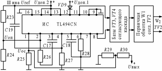
The voltage supplied to pin 12 (Fig. 101) of the IC chip from the rectifier to VD 9, not stabilized and serves for the initial start-up of this microcircuit. To generate a sawtooth voltage, the internal generator of the IC microcircuit between its pin 6 and the common wire of the secondary voltage is connected to a resistor R28 with a nominal resistance value, for example, 12 kOhm, and a capacitor C18 with a capacity of, for example, 1500 pF is connected between the common wire and terminal IC 5 (Fig. 100). According to the service documentation for the TL494 microcircuit, the calculation of the generation frequency, in relation to the elements of this schematic diagram, can be made according to the following formula:

With the indicated values of the elements of the RC chain, the frequency of the generator is ~ 55.5 kHz. Internal generator generates a signal with an increasing voltage, the shape of which is shown in the upper diagram in Fig. 101.
According to the technical documentation for the TL494 microcircuit, the voltage rise reaches the level of +3.2 V, after which the capacitor is discharged and the sawtooth voltage U 5 on it abruptly drops to zero. Then the process repeats cyclically (see diagrams in Fig. 101). The type of signals is of a qualitative nature and does not reflect real time and amplitude relationships.
The sawtooth voltage is applied to the inverting inputs of the "dead zone" comparator - the DA1 element and the PWM comparator - the DA2 element. An internal source of the initial bias is connected to the second input of the comparator, the value of which is set and is U 4 = 100 mV.
Diagram 1 fig. 101, the presence of this source is conventionally depicted by a straight line intersecting the "teeth" of the sawtooth voltage. The comparator is a threshold device, therefore, a signal is generated at its output, the values of which take on only two states. If the voltage at the inverting input exceeds the voltage level at the non-inverting input, then a low voltage is set at the output of the comparator, in this case zero. Conversely, if the voltage at the inverting input is less than at the non-inverting input, then the output voltage takes on a high level value, close to the supply level. In our case, when the voltage of the initial bias at the non-inverting input of the comparator DA1 is greater than the voltage of the sawtooth generator applied to the second input, the output voltage (diagram 2 in Fig. 101) has a high level. Discrete elements of the cascades are connected to the input of IC 4 only with a positive supply voltage. The offset at the non-inverting input DA1 by 100 mV is minimal, and the voltage increment at IC 4 can only increase it. Therefore, we can conclude that the duration of the pulses generated at the output of DA1, at a given initial offset, has a minimum value and with an increase in the voltage at the output of IC 4, the duration of the pulses of positive polarity will only increase. What effect this property has on the operation of the entire control scheme will be discussed below. A periodic sequence of pulses from the output of the comparator DA1 is fed to a digital logic element of the OR type - DD1. The pulse repetition rate is determined by the timing characteristics of the sawtooth voltage.
Diagram 3 fig. 101 shows the sawtooth voltage and the feedback voltage U 3, which, depending on the action of destabilizing factors, can vary (Fig. 100).
The error amplifier on the DA3 element compares the feedback voltage and the reference voltage, the level of the latter is determined by the ratio of the resistors R23 and R24 connected between the IC pin 14 and the common wire. 100. The internal stage of the IC circuit forms a stable voltage with a nominal value of +5 V at the IC 14 pin. Resistors R23 and R24 form a voltage divider, the midpoint of which is connected through the IC 2 pin to the inverting input of the DA3 operational amplifier. The non-inverting input DA3 through two resistors R29 and R30 receives voltage from the outputs of the secondary voltage channels with a value, for example, +5 V. Input ИС 1 is connected to the common wire of the secondary power supply through the resistor R25. The values of the resistances of the resistors R25 and R29, R30, forming the divider, are selected in such a way that at the nominal values of the output secondary voltages at the output of IC 1, a voltage is set slightly below the value of +2.5 V. This created some initial differential offset at the inputs of DA3. The DA3 amplifier operates in a linear mode, the gain parameters are determined by the internal circuitry of this stage. DA3 is powered only from an internal source with positive value voltage. Therefore, the change in the output voltage on DA3 can only occur in the positive region. To fulfill this condition, the voltage at the output of IC 1 should not exceed +2.5 V. Exceeding this threshold will lead to the fact that a voltage with a zero value will be established at the output of DA3. Further, we will assume that this does not happen, and the circuit operates in a certain range specified for the adjustment zone.
So, at the input of IS 2, the voltage is constant, and the input of IS 1 from the load receives a feedback voltage, which has a deviation determined by disturbing factors. At the output of the DA3 amplifier, a mismatch or error signal is generated, the accuracy of which is determined by the stability parameters of the internal reference voltage of the IC microcircuit. It is clear that all its deviations from the nominal value will be transmitted to IS 2. The output of DA3 is connected to the non-inverting input of the PWM comparator - DA2, a sawtooth voltage from the generator is supplied to its second input. The waveforms of various signals at the DA2 inputs are shown in diagram 3, shown in Fig. 101. The line crossing the "saw" shows the voltage at the non-inverting input DA2. Appearance the resulting signal at the output of DA2 is shown in diagram 4 (see Fig. 101). It can be seen that pulses of positive polarity are formed here in the case when the level of the voltage supplied from the output of DA3 exceeds the level of the linearly increasing voltage at the inverting input of DA2. Diagram 4 shows how the duration of positive pulses changes and, accordingly, the pause between them, depending on the voltage waveform at the output of DA3. The duration of the positive pulse increases as the level at the output of DA3 increases, that is, the pulse duration is directly proportional to the voltage level at the output of the mismatch amplifier.
The sequence of pulses is fed to the second input of the digital element DD1, the first input of which receives a pulse signal from the output of DA1 - the comparator of the "dead zone".
The elements of the IC microcircuit, the operation of which is described above, are included in the analog part of signal processing and formation. It should be noted that the comparators occupy a borderline position here. Receiving analog signals at the inputs, they form a two-level signal at the outputs. Components with letter designation DD relate to elements of exclusively digital automation, operating with discrete signals both at inputs and outputs. Signals have only two levels. In positive logic (we will continue to adhere to this terminology), the logical unit is considered to be the voltage value close to the level of the positive power supply. The logic zero level is a low level, close to the potential of the common wire.
The output state of the DD1 element, logical OR, takes the value of a logical unit if and only if at least one (arbitrary) of its inputs the signal also has a high logic level. The output is considered to be in a low level state when voltages of also low level are applied to all inputs of the OR gate.
The type of pulse output signals of the DD1 element is shown in diagram 5. The sequence obtained at the DD1 output is basic for the formation of the final control action on power elements power amplifier. All time relationships of the final signal are already embedded in this initial sequence. The output of DD1 is connected to the counting input C of the dynamic trigger - DD2, as well as to one of the inputs of each of the logical elements DD5 and DD6.
The state of the outputs of the dynamic trigger changes with the arrival of the positive edge of the pulse at its counter input. At this moment, the state of the information input, pin D, is "rewritten" (repeated) to the direct output of the trigger - pin Q. Output (-Q) always has a state opposite to Q (diagrams 6 and 7).
The functional diagram shown in Fig. 99 shows that the dynamic flip-flop DD2 (D-flip-flop) has an inverse output connection with the information input - D. Such a trigger connection sets it to the mode of dividing the frequency of the pulse sequence entering the counting input into two ... The trigger is triggered, that is, a change in the state of its paraphase outputs, occurs only when the positive edge of the pulse arrives at the input C. At this time, each of its exits changes its state to the opposite. Pins Q and D are connected, so any change in the state of output Q is transmitted to input D. As a result, each edge arriving at input C overwrites the changed level of input D to the outputs. Between the arrival of two edges, the state of the trigger outputs remains stable, as shown in Diagrams 7 and 6 (see Fig. 101). Diagram 7 corresponds to the state of the direct output of the flip-flop - pin Q, and diagram 6 - to the change in the state of the inverse output - pin (-Q). The trigger is switched on the positive edges of the sequence diagram 4.
The process of digitally dividing the original frequency by two has important feature: regardless of the type (timing of pulses and pauses) of the input pulse signal, in the sequence obtained as a result of division, the pulse and pause durations will be equal (see diagrams 7 and 6 in Fig. 101).
The output Q of the flip-flop DD2 is connected to one of the inputs of the element DD3, and the inverse output (-Q) is connected to one of the inputs of the logic element DD4. Two-input elements DD3 and DD4 perform the function of logical AND. Elements of this type form high logic level signals at the output pins when all their inputs also have high levels. With any other combination of logic levels at the inputs of the AND element, its output will remain low. All inputs of a logic element have the same effect on the formation of the output signal, that is, they are equal. If a high logic level is constantly applied to one of the inputs, then it will be permissive and will not affect the passage through the signal element from the second input. Otherwise, all changes to the signal set at the second input will be exactly repeated at the output.
In Fig. 100, the output of the IC 13 microcircuit is connected to one of the inputs of the DD3 and DD4 elements and can be used to block pulse signals arriving at the DD3 and DD4 elements from the DD2 trigger outputs. Blocking is performed by applying a low logic level signal to this pin. In this schematic diagram, Fig. 100. IC output 13 is permanently connected to IC 14 - the output of the internal reference voltage source. This potential is a constant resolution for passing the sequences from the flip-flop outputs to the DD3 and DD4 outputs. Consequently, the voltage waveform at the inputs and outputs of the elements, respectively, DD3 and DD4 will be identical (diagrams 9 and 8, (See Figure 101) In this case, these elements act as buffers and repeaters.
The last elements installed in the PWM signal shaping circuit are two-input elements DD5 and DD6. One input of these elements is connected to DD3 and DD4, respectively, and the other pair of inputs of elements DD5 and DD6 are combined with each other and connected to the output of DD1. Elements DD5 and DD6 are used to execute a logical function of the OR-NOT type. These elements perform a logical operation similar to DD1, but they also add negation, which in digital technology is equivalent to inversion. A low-level signal appears at the output of the OR-NOT gate when a high-level voltage is set at at least one of its inputs. If a two-input OR (OR-NOT) element has some abstract difference between the inputs and one is considered as informational, and the second - as allowing, then we can conclude that for the passage of data from the first input to the output of the element at the input, there must be the voltage is set to low. When a high level is applied to the enable input, the information is blocked, and a low level is constantly present at the output. This is true for the logic of the element of the OR-NOT type.
At the DD5 input, the signals coming from the DD1 outputs act (see diagram 4 in Fig. 101 and DD3 (see diagram 7). As a result of the logical addition of these input influences with the inversion at the output of the DD5 element, the signal shown in diagram 8 appears. the shape of the pulses received at the output of element DD6 is shown in diagram 9. Pulses of positive polarity arrive at the outputs of DD5 and DD6 when both input signals for each of these elements take a low level value.
Diagrams 4, 8 and 9 show that at the outputs of DD5. and DD6, alternating pulses of the sequence of diagram 4 appear. Working pulses in diagram 4 will be considered time intervals, the boundaries of which are outlined by the fall and the front, that is, the beginning of the pulse is the decline of the positive voltage, and its end is the positive edge. One pulse from the DD1 output is fed to the output of the DD5 element, and the input signal to DD6 is blocked at this moment high level supplied from the inverting output of the flip-flop DD2. The next pulse from the sequence at the DD1 output appears already at the DD6 output, and in DD5 it is blocked by a high level coming from the direct output of the DD2 trigger. At the output of each of the logical elements DD5 and DD6, pulses appear alternately from the sequence formed at the output of DD1.
At the outputs DD5 and DD6, two pulse trains are formed. The pulse repetition rate in each of them is two times lower than the frequency of the sawtooth voltage across the capacitor C18. The positive-polarity pulses of the two sequences are spaced in time, that is, their action intervals do not overlap. Further, each sequence is used to control its own half-bridge switching power amplifier transistor. The issue of correct formation of pulse sequences for excitation is quite important. transistor circuit power amplifier, therefore it is necessary to consider some boundary cases of the operation of the power supply circuit and the response to them of the elements of the IC microcircuit.
The temporal position of the pulses is rigidly determined by the shape of the sawtooth voltage. The slopes of the pulses in each of the sequences are synchronized with the slopes of the ramp voltage generated by the microcircuit generator. The time position of the fall is not changed. If we look at diagram 3, we can note that the position of the decay of the pulse generated by the PWM comparator (see diagram 4) depends on the current ratio of the "saw" voltage and the mismatch voltage. A decrease in the level of the mismatch voltage in diagram 4 causes a "shift" of the beginning of the pulse to the left. The position of the front of this impulse, that is, its end, is rigidly determined by the moment of the decay of the sawtooth voltage, therefore, its duration increases. The frequency of the pulses does not change, and their duration is regulated by the output level of the DA3 mismatch amplifier.
At the beginning of the description of the operation of the PWM converter, the so-called "dead zone" comparator was mentioned (see diagrams 1 and 2). Now that it became clear general mechanism operation of the entire circuit of a pulse-width modulator, it should be explained the need for its presence in circuits of this type.
On element DD1, the logical addition of pulse signals from the comparators DA1 and DA2 is performed. Previously, it was assumed that the positive pulse of the DA2 comparator is wider than the analogous output pulse from DA1. However, if the process of pulse narrowing from DA2 begins, then at zero level signal from DA1 in the extreme case at the output DD1 will establish a constant low level. Trigger DD2 will not be able to switch its outputs, and constant opposite logic levels will appear on DD5 and DD6. This will stop the process of switching the power stage transistors. To protect against the occurrence a similar situation a "dead zone" comparator is intended. With the narrowing of the pulse from DA2, a moment comes when the duration of the positive pulse from DA1 becomes decisive when the signals arriving at the DD1 inputs are added. A positive pulse at the output of DD1 cannot be "narrower than the output pulse of the comparator of the" dead zone. " whose durations will coincide with pauses (logical zeros) in diagram 2. The pause between these pulses will be equal to the duration of positive pulses in diagram 2. This means that the node on the comparator of the "dead zone" is guaranteed to ensure the appearance of the sequence converter in the output stages of the PWM pulses with specified intervals of pauses between pulses.This mechanism of action allows you to increase the flow of energy into the secondary circuit and resume the process of PWM regulation using the amplifier DA3 and comparator DA2. power transistors of the power amplifier.
The appearance of pulse signals at the outputs of elements DD5 and DD6 ends the logical processing of the error signal and the formation of PWM sequences in the converter. The appearance of these pulse trains will remain unchanged until they are applied to the power elements of the power amplifier. All stages installed between the outputs of the elements DD5, DD6 and the base circuits of the power amplifier transistors are intended only to increase the energy characteristics of control pulses and match their levels.
Internal transistors VT1 and VT2 of the IC chip are used for the primary amplification of control sequences of pulses, which are fed to their bases (see diagrams 10 and 11, Fig. 101) from elements DD5 and DD6. The terminals of these transistors do not have internal connections to any load resistive circuits. They are specially left free for the use of transistors in different options inclusion schemes.
Direct connection of the TL494 output transistors to a power transformer is rarely used. Usually, an intermediate amplification stage is used, built on transistors, for example, of the 2SC945 type. In this case, the emitters of transistors VT1 and VT2 of the microcircuit (9,10) are interconnected, and their collectors (8 and 11) have a transformer connection with the power amplifier. This is a traditional approach to the formation of matching circuits of a low-voltage, relatively low-power control unit and a high-voltage power stage. The implementation of this approach boils down to the following. Voltage pulses of a rectangular shape (see diagrams 12.13, Fig. 101) on the collectors of transistors VT1 and VT2 are fed to the bases of two transistors (they are not shown in Fig. 100), the collectors and emitters of which are included in the primary winding (circuit with a midpoint ) low-power matching high-frequency transformer TV2. Voltage pulses of rectangular shape from the secondary winding of this transformer are fed to the input of powerful transistors included in the primary winding of the power transformer TV1 (midpoint circuit), from the secondary winding of which the voltage (s) flows through the rectifier (s) and smoothing ( f) filter (s) to consumers of electrical energy.
Thus, the considered stage serves to amplify the level and power of the pulse signals of the IC (diagrams 12, 13, Fig. 101), to a level sufficient to start a half-bridge (or made according to another scheme) amplifier and maintain the voltage on consumers within a given at the action of disturbing factors.
In pulsed IVEP, transistors of the 2SC945 type or their functional analogs are often included in the primary winding of the TV1 power transformer. They are used very widely, regardless of the manufacturer of the product. Limit values major technical parameters these transistors are as follows:
· Maximum dissipation power - 250 mW;
Collector-base voltage - 60 V;
· Collector-emitter voltage - 50 V;
· Emitter-base voltage - 5 V;
Collector current - 100 mA;
Base current - 20 mA;
· Typical value of the gain in the circuit with a common emitter - 185-200;
· Typical capacitance of the collector-base junction - 3 pF;
· The typical value of the unity gain frequency f t is 250 MHz.
According to the domestic classification, they belong to the family of transistors high frequency and low power.
Miracles of Altai. People were so carried away by foreign resorts that they forgot that our country is much larger than the whole of Europe. For example, the territory of Gorny Altai, whose area is 9, 2 thousand km2, can accommodate ten Great Britain. And only 200 thousand people live on its territory. So it turns out that for secrets and mysteries this is the most the best place... And if you feel like touching ancient history and get acquainted with the real secret, then you are here. Valley of the Dead. History and a large number of free space allowed for the preservation of amazing monuments. For example, in the Chemal region there is a whole "valley of the dead". The banks of the Katun River and its tributaries are dotted with thousands of Scythian burial mounds, most of which have not yet been excavated. This is an amazing sight. But modernity interferes even in seemingly inviolable places. In the near future, it is planned to resume the construction of the Katunskaya hydroelectric power station. The resulting reservoir threatens to flood a significant number of mounds, so now Russian and Altai archaeologists are trying to speed up their work. The oversaturation with graves gives rise to numerous conjectures as to why there were so many of them in Altai. According to one of them, this land was the ancestral home of all mankind. More modest scientists agree that Altai is the ancestral home of the Indo-European race. There is a version that this was the center of a powerful Scythian state, whose borders reached the Danube. There are indeed many artifacts of the famous Scythian "animal style" dating back to the 13th century BC. - III century A.D. They say that the sacred land of Altai magically she did not let her sons go, and they, subject to her charms, brought the dead (wherever death overtook them) exactly here, to their historical homeland. Miracles. There are mountain ghost people. Miracles. They lived a long time ago and came from the Emond steppe. They were the masters of Altai. Their disappearance has something to do with white. One theory somehow ties white birch... Roerich's theory says that the disappearance of this people is associated with the appearance of white people. Allegedly, the Chudi refused to obey. Nevertheless, the Chudi disappeared and disappeared in a very interesting way - they buried themselves: Chudi dug large holes, made a flooring of the earth, supported wooden racks, went there with the whole tribe and brought down the "roof" on themselves. In place of these self-burials, over time, conical pits form, into which people sometimes fall. There is a hypothesis that in this way the Chudi tried to go to another, parallel world... And they succeeded. There are people (climbers, rock climbers) who claim to have seen some creatures, similar to people, who came out of the rocks and went back there. Although, these visions could be the result of altitude sickness.
Rice. 40
Rice. 39
Rice. 38
Rice. 37
Note - more details about the microcircuit itself and the principle of its operation are shown further in paragraph 2.4.2. - PWM regulator on IC TL494.
Switching voltage regulators on IC TL494.
The sawtooth voltage is often obtained from a separate device - the sawtooth voltage generator (RVG).
The frequency of the sawtooth voltage is determined RC chain and usually f gpn = const, but, if necessary, changing the parameters RC you can set (adjust) the required frequency.
It is known that the switching frequency of the switching device is transistors VT 2, VT 3 in the ISN with PWM is constant (it is set by the FPG). Under the influence of destabilizing factors, the voltage across the external resistor changes R 9 and, accordingly, at the output of the differential amplifier U ypt, which leads to a change in duration open state transistors VT 2, VT 3 regulators, and the voltage at the output of the switching regulator remains unchanged.
3.7.3 PWM controllers TL494 series
Currently, microcircuits (domestic and imported) are widely represented on the market, which implement a different set of PWM control functions for specific tasks... PWM controllers of the TL494 series (domestic analogue of KR1114EU4) have proven themselves well. Their detailed description given in. These microcircuits provide enhanced capabilities in the development of IVEP and implement a full set of PWM control functions. The microcircuit carries out the formation of a reference voltage, amplification of the error signal, the formation of a sawtooth voltage, PWM modulation, the formation of a push-pull output, protection against through currents and overloads, external synchronization, wide range adjustment, provides a soft start and the possibility of external activation.
main parameters and characteristics of the TL494 microcircuit:
· Supply voltage Ucc - 7 ... 40 V;
Voltage on closed collectors key transistors no more than 40 V;
· Current of output key transistors - 250 mA;
· Reference voltage - 5 V ± 5%;
· general power dissipation in continuous mode (package DIP-16.<25 ºС) – не более 1000 мВт;
Operating range of ambient temperatures:
· With suffix L - from -25 ... + 85 ºС;
· With suffix С - from 0… + 70 ºС.
· Current through the feedback output - no more than 0.3 mA;
· The capacity of the timing capacitor St - 0.047 ... 10000 nF;
· Resistance of the timing resistor - 1.8..500 kOhm;
· Generator frequency - 1 ... 300 kHz;
· Current consumption of the microcircuit - no more than 20 mA;
· Front of the output current pulse - no more than 200 ns;
· Decay of the output current pulse - no more than 100 ns.
In addition, the independent output drivers of the transistor microcircuit provide the ability to operate the output stage according to a common emitter circuit or an emitter follower circuit.
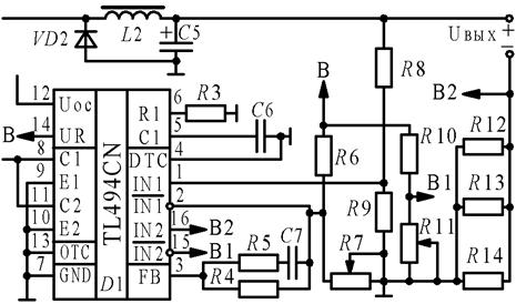
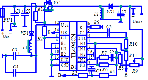
3.1.1 Circuit diagram of a pulsed buck
stabilizer on IC TL494
In the proposed rice. 37 stabilizer, the maximum input voltage is 30 V, it is limited by the maximum allowable drain-source voltage of the p-channel field-effect transistor VT 1 RFP60P03 from Mitsubishi Electric. Resistor R 3 and capacitor WITH 6 set the frequency of the internal sawtooth voltage generator, it is determined by the formula

On rice. 37 indicated: VD 1-KD212A; VD 2-2D2998B; VT 1-RFP60PO3; C 1, C2-2200μ × 40V; C 3-10 microns × 63V; C 4-0.1mk; C 5-1000 μ × 25V; C 6-4700;C 7-0.1 microns; FU 1-MF R400; R 1-200 Ohm, 0.125 W; R 2-510 Ohm, 0.5W; R 3-30 kOhm, 0.125 W; R 4-1 M, 0.125 W; R 5-47 kOhm, 0.125 W; R 6-4.7 kΩ, 0.125 W; R 7-4.7 kΩ; R 8-5.6 kOhm, 0.125 W; R 9-1 kOhm, 0.125 W; L 1-80 μH; I-6 A; U in = 24 V; U out = 0 ... 11 V.
From a reference voltage source (pin 14) through a resistive divider R 6, R 7, a part of the reference voltage is applied to the inverting input of the error amplifier # 1 (pin 2). Feedback signal through a divider R 8, R 9 is fed to the non-inverting input of the error amplifier (pin 1) of the microcircuit. The output voltage is regulated by a resistor R 7. Resistor R 5 and capacitor WITH 7, the error amplifier is frequency corrected.
It should be noted that independent the output formers of the microcircuit ensure the operation of the output stage in both push-pull and single-pull modes. In the stabilizer, the output driver of the microcircuit is switched on in a single-cycle mode. For this, pin 13 is connected to a common wire. Two output transistors (collectors - pins 8, 11; respectively, emitters - pins 9, 10) are connected according to the scheme with a common emitter and work in parallel. In this case, the output frequency is equal to the generator frequency. The output stage of the microcircuit through a resistive divider R 1, R 2 controls the key element of the FE stabilizer - the field-effect transistor VT 1. In the power circuit of the microcircuit (pin 12). To suppress various high-frequency interference and more stable operation of the stabilizer as a whole, the LC-filter on elements L 1, C 3, C 4. As can be seen from the schematic diagram of the stabilizer, when using the TL494 microcircuit, a relatively small number of external elements is required.
A self-healing fuse is used to protect the stabilizer from overcurrent. FU 1 MF-R400 from Bourns. The principle of operation of such fuses is based on the property of sharply increasing their resistance when a certain threshold value of the current or ambient temperature is exceeded and automatically restoring their properties when these reasons are eliminated. Below are the specifications for the above fuse:
· Maximum operating voltage - 30 V;
· Maximum current, which does not lead to a change in the parameters of the fuse - 4 A;
· Current, which leads to a jump in resistance - 8 A;
· Operating temperature range - from -40 to +85 ºС.
It was possible to reduce switching losses and increase the efficiency of the stabilizer thanks to the use of a Schottky diode ( VD 2) KD2998B with parameters:
· Constant forward voltage - 0.54 V;
· Average forward current - 30 A;
· Frequency range without reduction of electrical parameters –10..200 kHz;
Pulse reverse voltage - 30 V.
The main technical characteristics of the buck stabilizer (fig. 37)
· Input voltage - 24 V;
· Output voltage - 0 ... 11 V;
· Maximum load current - 6 A;
· Amplitude of output voltage ripple - no more than 100 mV;
· Instability of the output when changing the load current and ambient temperature - no more than 1%;
· Average value of efficiency at maximum load current in the entire range of output voltage - about 90%;
It was experimentally found that the stabilizer has a maximum efficiency (≈90%) at a frequency of 12 kHz, but at an output power of about 40 W, a barely noticeable whistle is observed. The whistle disappears if you increase the conversion frequency to 20 kHz (with a decrease in efficiency by 2 ... 3%). The efficiency at an output power of up to 10 W (U out = 10 V) reaches 93%.
The L2 choke is wound on two MP-140 K24 × 13 × 6.5 annular magnetic circuits folded together and contains 45 turns of PETV-2 wire with a diameter of 1.1 mm, laid evenly in two layers along the entire perimeter of the ring. Between the layers, two layers of lacquer cloth LShMS-105-0.06 GOST 2214-78 should be laid. The inductance of the choke is 220 μH. Resistors - C2-33N. Capacitors WITH 1, WITH 2, WITH 3, WITH 5 - K50-35, WITH 4, WITH 6, WITH 7 - K10-17. Variable resistors - SP5-3 or SP5-2VA. Chip TL494CN can be replaced with TL494LN or KR1114EU4. Throttle L 1 - DM-0.1 with inductance 80 μH. The self-resetting fuse of the MF-R series can be matched to each specific case. Diode VD 2 can be replaced with any other Schottky diode with parameters no worse than the above, for example 20TQ045.
In the stabilizer, the overcurrent protection unit can be made differently. The TL494 has an error amplifier # 2 (inverting I / O 15, not inverting I / O 16). The outputs of both error amplifiers are active high and are OR-coupled at the non-inverting input of the PWM comparator. In this configuration, the amplifier that takes the shortest time to turn on the output is dominant in the gain loop.
A fragment of the stabilizer circuit with an overcurrent protection unit is shown on rice. 38 .
Parallel resistors R 12-R 14 acting as a current sensor are connected in series with the load. The voltage from the current sensor is fed to the non-inverting input (pin 16) of the error amplifier No. 2. The current threshold (voltage at the inverting input of the amplifier, pin 15) in the load is set by the divider R 10, R 11.
On rice. 38 indicated: VD 2-2D2998B; C 5-1000 μ × 25V; C 6-4700;C 7-0.1 microns; R 3-30 kOhm, 0.125 W; R 4-1 M, 0.125 W; R 5-47 kOhm, 0.125 W; R 6-4.7 kΩ, 0.125 W; R 7-4.7 kΩ; R 8-5.6 kOhm, 0.125 W; R 9-1 kOhm, 0.125 W; R 10-4.7 kΩ, 0.125 W; R 11-270 Ohm; R 12, R 13, R 14-0.1 kOhm, 1 W; L 1-80 μH; I-6 A; U out = 0 ... 11 V.
As soon as the current in the load exceeds the set threshold value and the error amplifier # 2 of the microcircuit is dominant in the control loop, the stabilizer will start operating in the current stabilization mode. If the load current is less than the threshold value, the stabilizer will return to the voltage stabilization mode. To reduce power losses, the current sensor is made with a minimum resistance of 0.03 Ohm: at a maximum load current of 6 A, the power dissipated on the sensor
is only 1.08 watts. Resistors R 12...R 14 - type C5-16MV 1 W, 0.1 Ohm ± 1%. Resistor R 11 - SP5-3 or SP5-2VA. If necessary, to reduce losses, the resistance of the current sensor can be further reduced.
The stabilizer is made on a board with dimensions of 55 × 55 mm. During installation, it is advisable to separate the common wire of the power section of the stabilizer and the common wire of the microcircuit and connect them at the output of the stabilizer, as well as minimize the length of the conductors (especially the power section).
The transistor is installed on a radiator with an effective surface area of at least 110 cm 2. The stabilizer, with proper installation, does not need to be adjusted. In a stabilizer with an overcurrent protection unit (Fig. 38), it is necessary to set the voltage at pin 15 of the microcircuit, which is calculated by the formula: U 15 = I × R, where I is the maximum load current; R- resistance of the current sensor.
Initially no load with a resistor R 11 it is necessary to set the required voltage U for the maximum load current (for the current I por = 8 A, U = 0.24 V). It is better to turn on for the first time at a load of 0.2 ... 0.4 A. Then slowly increase the output voltage to the maximum value and then, increasing the load current, check the transition of the stabilizer to the current stabilization mode.
Instead of the RFP60P03 transistor, a cheaper RFP10P03 can be used, but the use of a cheaper element base may lead to a deterioration in the technical characteristics of the stabilizer.
3.1.2 Principle diagram of a pulse boost
stabilizer on IC TL494

In some cases, it is necessary that the output voltage of the stabilizer be higher than the input voltage. On rice. 39 the block diagram of a pulse parallel boost-type regulator is shown.
In this switching regulator, when the FE key element is open, the current from the source U inlet flows through the throttle L 1, storing energy in it. Diode VD 1 is closed at the same time. The current into the load during this period of time comes only from the capacitor WITH 1 .
On rice. 39 indicated: VD 1-KD212A; VD 2-2D2998B; VT 1-IRFP540; C 1, C2-2200μ × 40V; C 3-10 microns × 63V; C 4-0.1mk; C 5, C 6 - 3300 μ × 63 V; C 7-4700; WITH 8-0.1 microns; WITH 9-1000 μ × 25 V; FU 1-MF R400; R 1-1 kOhm, 0.25 W; R 2-750 Ohm, 0.25 W; R 3-30 kOhm, 0.125 W; R 4-1 M, 0.125 W; R 5-47 kOhm, 0.125 W; R 6-4.7 kΩ, 0.125 W; R 7-4.7 kΩ; R 8-150 kOhm, 0.125 W; R 9-4.7 kOhm, 0.125 W; L 1-80 μH; I-1.4 A; U in = 24 V; U out = 26.5 ... 50 V.
The next moment, when the FE closes, the choke energy L 1 is given to the load. In this case, the output voltage will be greater than the input voltage. Unlike the buck stabilizer ( rice. 38 ) here the choke is not a filter element, and the output voltage becomes greater than the input voltage by an amount that is determined by the inductance of the choke L 1 and the duty cycle of the key element of the FE.
In the stabilizer on rice. 39 applied, basically, the same radioelements as in the previously considered one.
Main technical characteristics of the boost stabilizer:
· Input voltage - 24 V;
· Output voltage - 26.5 ... 50 V;
· Maximum load current (at U out = 50 V) - 1.4 A;
· Amplitude of output voltage ripple - no more than 200 mV;
· Instability of the output when changing the load current and ambient temperature - 1.5%;
· Average value of efficiency at maximum load current in the entire range of output voltage - about 9.2%;
· Conversion frequency - 15 kHz;
· Operating temperature range - from -25 to +85 ºС;
· The amplitude of the stabilizer output voltage ripple at maximum load is about 200 mV.
The ripple can be reduced by increasing the capacity of the output filter. For a "softer" start, a capacitor is connected between the common wire and the non-inverting input of the error amplifier # 1 (pin 1) WITH 9. To protect the stabilizer from overcurrent, you can use the functional unit shown in fig. 38.
Throttle L 2 is the same as in the buck regulator circuit, VT 1 - n-channel field-effect transistor IRF540 with parameters: U si = 100 V, I s u = 28 A, R si = 0.077 Ohm (maximum values). Resistors - C2-33N. Capacitors WITH 1, WITH 2, WITH 3, WITH 5, WITH 6, WITH 8, WITH 9 - K50-35; WITH 4, WITH 7, WITH 8 - K10-17. Variable resistors - SP5-3 or SP5-2VA. Transistor VT 1 should be installed on a radiator with an effective surface area of at least 100 cm 2. You can use a cheaper n-channel field-effect transistor, of course, with some deterioration in the technical characteristics of the stabilizer. It is better to turn on the first time with a small load of 0.1 ... 0.2 A and a minimum output voltage, then slowly increase the output voltage and load current to maximum values.
If the boost and buck stabilizers operate from the same voltage source, then their conversion frequency can be synchronized. In the diagram of synchronization of two TL494 microcircuits is shown. To do this, in the slave stabilizer, you need to remove the timing resistors and the capacitor and close pins 6 and 14 of the microcircuit, and connect the pins 5 of the microcircuits of both stabilizers to each other.
In the stabilizer of the step-up type, the choke L 2 does not participate in smoothing the ripple of the output DC voltage. In step-up stabilizers for high-quality filtering of the output DC voltage, it is necessary to use output filters with sufficiently large values L and WITH... This leads to an increase in the mass and dimensions of the filter and the device as a whole. Therefore, the specific power of the buck regulator is greater than that of the boost regulator.
3.1.3. Schematic diagram of a pulse
inverting regulator on IC TL494
A schematic diagram of a pulse inverting stabilizer is shown on rice. 40. This ISN is made according to the scheme given in chapter 2, §2.2.3.
Also, as in the step-up stabilizer, the choke when the FE is open accumulates energy, and when it is closed it gives it to the load, however, due to the different order of connecting the elements, the stabilizer has the property of inverting the polarity of the output voltage relative to the input voltage.
On rice. 40 indicated: VD 1-KD212A; VD 2-2D2998B; VT 1-RFP60PO3; C 1, C2-2200μ × 40V; C 3-10 microns × 63V; C 4-0.1mk; C 5-1000 μ × 25V; C 6-4700;C 7-220 μ × 40 V; WITH 8-0.1 microns; FU 1-MF R400; R 1-200 Ohm, 0.125 W; R 2-510 Ohm, 0.5W; R 3-1 kOhm, 0.125 W; R 4-4.7 kOhm, 0.125 W; R 5-30 kOhm, 0.125 W; R 6-1 MΩ, 0.125 W; R 7-47 kΩ; R 8-1 kOhm, 0.125 W; R 9-10 kOhm, 0.125 W; R 10-1 kOhm, 0.125 W; R 11-5.6 kOhm, 0.125 W; L 1-80 μH; I-4.5 A; U input = 24 V; U out = 0 ... 11 V.
In the inverting stabilizer, basically the same electronic components are used as in the previously described ones.
Main technical characteristics of the inverting stabilizer:
· Input voltage - 24 V;
· Output voltage - 11 V;
· Maximum load current - 4.5 A;
· Amplitude of output voltage ripple - no more than 150 mV;
· Instability of the output when changing the load current and ambient temperature - 15%;
· Average value of efficiency at maximum load current in the entire range of output voltage - 80%;
· Conversion frequency - 15 kHz;
· Operating temperature range - from -25 to +85 ºС.
In order to eliminate the inrush of the input current, especially when operating at a large load, a "soft" start is implemented in the stabilizer by introducing R 3 and WITH 5.
Transistor VT 1 should be installed on a radiator with an effective surface area of at least 140 cm 2. Diode VD 2 is also installed on a radiator with an effective surface area of at least 10 cm 2.
The input voltage of the stabilizers can be reduced or increased if we take into account all the above requirements for each stabilizer, but the current must be re-calculated the divider R 1, R 2 so that the divider current and the source-gate voltage of the transistor VT 1 have not changed. ?????
The KR142EP1 pulse control microcircuit ensures the operation of the ISN mainly in a relay on-off mode, but the IC also provides the ability to create a voltage stabilizer with pulse-width modulation.
For example, if, for one reason or another, it is required that the operation of the threshold device be synchronized with the frequency of any external device, then its synchronizing signal is fed to the pin. 14 and 15 IS. Often, a square-wave generator - a master oscillator - is used as such a device. The alternating voltage of a rectangular shape of such a generator using a differentiating RC chains converted to sawtooth voltage U drank. In this case, the resistor is used R 10 microcircuits, and an external capacitor is used with a small capacity.
Diodes are used as an input unit for this signal. VD 3...VD 6 connected between the differential amplifier and the Schmitt trigger. Thus, across the resistor R 10, a comparison of two voltages is carried out - the first is proportional to the change in voltage across the load (as in the IMS with the RE) and it is removed from the collector VT 11 differential DC amplifier U ypt, and the second is a sawtooth voltage U drank. As a result of comparing these voltages, an error signal is allocated, which is fed to the inverting stage VT 7.
The sawtooth voltage must have sufficient swing to translate VT 7 into saturation state. The latter, in the open state, operates in a mode close to saturation. Delay of the moments in time at which VT 7 goes out of saturation, with respect to the leading edge of the sawtooth voltage depends on how open the transistors are VT 7,VT 8. If the transistors are almost locked, and the average voltage between their base and emitter, given by the collector potential VT 8 is small, then it will be equal to the linearly decreasing voltage at the output of the rectifier only at the end of the cycle.
With increasing potential on the collector VT 11 (i.e., with increasing voltage across the load), the voltage also increases U pack. This voltage corresponds to a long pause between voltage pulses (shorter voltage pulse duration) taken from the total emitter load of transistors VT 7,VT 8 - R 9(U B VT 6) microcircuits.
Transistors VT 6, VT 5, VT 4 are amplifiers of pulses taken from the resistor R 9. Amplified pulses from the collector VT 4 through an external voltage divider ( R 6, R 3) are fed to the base VT 3, which is one of the transistors of the switch included in the IC. This key ( VT 2, VT 3) in this circuit, the ISN controls an external power switch, also made in the form of a composite transistor ( VT 2, VT 3). Thus, with an increase, for example, the supply voltage at the input of the ISN, the voltage U n = (t and / T) U n at the load will remain unchanged since the on-state time of the regulating transistor of the power section has decreased.