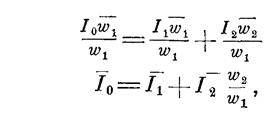
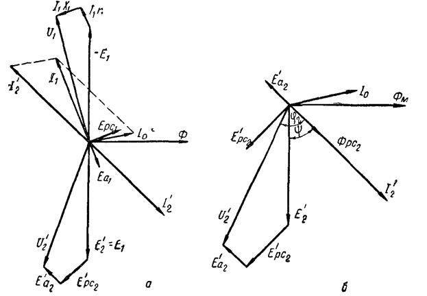
As you know, when the transformer is idle, current I flows in the primary winding 0 , which creates md with. I 0ω 1, and this ppm creates the main magnetic flux F and the scattering flux Ф рс1. Main magnetic flux F induces in the windings of the transformer e. etc. with. E 1 and E 2. If to the terminals of the secondary winding of the transformer Oh connect a load with a resistance z ng, then a current I 2 will flow through the secondary winding, lagging behind the emf. with. E 2 by the angle ψ (Fig. 92, a).
Fig 92 Transformer operation under load:
a - circuit diagram loaded transformer,
b - vector diagram of the ppm transformer
Multiplying the current I 2 on the number of turns of the secondary winding ω 2, we get the vector m. s. secondary winding I 2ω 2, which we postpone in the direction of the current vector I 2, as well as p.m. with. at idle I 0ω 1 (Fig. 92, b).
When a load current appears in the secondary winding, the current in the primary winding correspondingly increases, where instead of the current I 0 a current I 1 flows, creating a ppm. I 1ω 1 . According to formula (77), e. etc. with. primary winding E 1 = = 4,44 f 1 ω 1 F m. Ignoring the voltage drop across the primary winding, suppose that
If the voltage and frequency in the network are constant in magnitude, then the following equality can be written:
But in the formula 4.44, f 1 and ω 1 are constant numbers, therefore, with a constant voltage and frequency in the network, the magnetic flux of the transformer will be constant and will not depend on the load, i.e.

This equation is called the m.f. equation. transformer. M. d. S. transformer at idle I 0ω 1 and in the secondary winding I 2ω 2 plotted on the diagram.
From the equation of m.d.s. we define m. d. s. primary winding, it is equal to:
that is, to obtain m. from. primary winding I 1ω 1 you need to m. s. idle move I 0ω 1 add ppm secondary winding I 2ω 2 with the opposite sign, that is, by turning the vector of this md. 180 °.
Adding the vectors of these m.d.s, we get the m.d.s. primary winding I 1ω 1 (Fig. 92, b). As you can see from the vector diagram, p.m. with. the primary winding magnetizes the core of the transformer, and p.m. c. the secondary winding demagnetizes it. Geometric sum of vectors m.d.s. the primary and secondary windings gives the vector of the resulting ppm, which is equal to ppm. transformer at idle I 0ω 1 and creates a magnetic flux F.
You can also consider the issue in such a way that m. the primary winding creates a magnetic flux Ф 1, a magnetizing transformer, and p.m. with. of the secondary winding, the magnetic flux Ф 2, demagnetizing it, as a result, a magnetic flux Ф is formed in the core.
Primary current I 1 also creates a magnetic leakage flux Ф РС1, the lines of force of which do not interlock with the secondary winding, but are closed in the air, and the current of the secondary winding I 2 creates similarly the magnetic leakage flux Ф рс2.
Let us divide both sides of the m.d.s. equation. transformer at ω 1 :
The quantity is called the reduced current.
Let's consider what the reduced value is and what is the purpose of the reduction.
Since the number of turns of the primary and secondary windings of the transformer are different, then e. etc. with. and the currents in these windings are also not the same. They differ in k or in 1 / k once.
Therefore, it is impossible to compare these quantities or build vector diagrams where the values of the secondary and primary windings need to be added, just as it is impossible to add the distances measured on maps of different scales without bringing them to the same scale.
For example, it would not be possible to obtain the magnitude of the voltage drop in a loaded transformer by directly summing the voltage drops for each of the windings. Since these windings have currents and resistances of different magnitude, then the vectors expressing the magnitude of the voltage drops are not the same in magnitude for each winding.
In transformers, the values of the secondary winding lead to the primary in the same way as the distances measured on maps of different scales lead to the same scale, that is, a conventional transformer is replaced with a reduced one, in which the number of turns of the primary winding ω 1 is equal to the number of turns of the secondary winding ω 2 or k = 1. The given values are indicated by a prime at the top. To bring e. etc. with. it must be multiplied by the transformation ratio, since in the secondary winding it is k times less
 (83)
(83)
Voltage and other e. Are given in the same way. etc. with. in the transformer.
When bringing the current, the condition is met that the apparent power of the secondary winding after bringing does not change, i.e. E 2 I 2 = E 2 '. I 2 ' From here
 (84)
(84)
that is, to bring the current, it must be divided by the transformation ratio.
When reducing the active resistance, one proceeds from the condition that the losses in copper of the reduced transformer do not change
 (85)
(85)
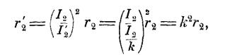
that is, to bring the active resistance, it must be multiplied by the square of the transformation ratio.
Because E pc2= I 2 x 2, then
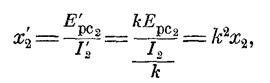 (86)
(86)
i.e. similarly with active resistance.
therefore, to bring any resistance, it must be multiplied by the square of the transformation ratio.
Let's build a vector diagram of a transformer with an active-capacitive load. In this case, the current is ahead of the e. etc. with. by an angle ψ 2. The construction is carried out as for a vector diagram with an active-inductive load.
Rice. 94. Vector diagram of the transformer with active-capacitive load:
a - full, b- for the secondary winding.
As can be seen from the diagram (Fig. 94), in this case, with an increase in the load, the voltage at the terminals of the secondary winding of the transformer increases.
To consider the processes occurring in transformers, an equivalent circuit is used. In the equivalent circuit, each transformer winding is replaced with real active and inductive resistances that it possesses, and an ideal winding without resistance. In addition, we assume that the action of e. etc. with. dissipation is equivalent to voltage drops across the inductive resistances of the transformer windings, and the effect of e. etc. with. active resistances - voltage drops across the active resistances of the windings.
Thus, the primary winding consists of real resistances x 1 and r 1 and ideal winding z 1 M, and the secondary, respectively, from x "2, r" 2 and Z "2 M (fig. 95, a). The windings z 1 m and Z "2 m are electromagnetically connected to each other by means of magnetic flux F m, creating in the windings of the transformer e. etc. with. E 1 and E "2.
Since we are considering a reduced transformer, in which ω 2 = ω 1 and k = 1, we can replace the electromagnetic connection with an electric one, combining the windings z lM and z ’2 m into one z 12, through which the current flows,
The winding z 12 is called a magnetizing winding, or a magnetizing branch, in which a magnetic flux is created F m current I 0 (Fig. 95, b). The voltage at the terminals of the magnetizing winding is E 1 = E "2.
This equivalent circuit corresponds to the complete vector diagram of the transformer (Fig. 93).
The equivalent circuit of the transformer and, accordingly, the vector diagram can be simplified. For this purpose, the magnetizing current I 0 is neglected, since it does not exceed, on average, 5% I H for most transformers, and the magnetizing branch of the equivalent circuit z 12.
Then the simplified equivalent circuit will consist of series-connected resistances r 1, x 1 and r "2, x 2, through which the current flows I 1, since in the given transformer the current I 1= I 2, if we neglect the no-load current.
To the clamps OH in the equivalent circuit, the voltage U 1 is supplied, and at the terminals Oh we get stress U "2, which is less U 1, by the amount of voltage change


Rice. 95. Equivalent circuit of the transformer under load:
a - transformer circuit, b - transformer equivalent circuit;
c - simplified equivalent circuit, d - simplified vector
diagram
due to the voltage drop in the transformer windings from the load current I 1 (fig. 95, v).
We construct a simplified vector diagram of the transformer corresponding to this equivalent circuit based on the same considerations - we neglect the idle current vector, and rotate all secondary vectors by 180 °. Current vector I 1 = I "2 we draw vertically, then at an angle φ 2 we postpone the voltage vector U "2(fig. 95, G). The voltage drop across the active resistance of the secondary winding I "2 r " 2 , and perpendicular to the current vector is the voltage drop across the inductive resistance of the secondary winding I "2 x "2 - Trailing vector OA is the vector e. etc. with. E 1= E "2.
Rice. 96. Simplified equivalent circuit of the transformer under load:
a - equivalent circuit; b - simplified vector diagram.
From the end of the vector e. etc. with. we postpone the voltage drop vector on the active resistance of the primary winding I 1 r 1 , and perpendicular to the current vector - on inductive I 1 x 1 . Vector OV- mains voltage U 1.
Voltage drops across the active resistances of both windings can be combined, the same can be done with the ratio of voltage drops across the inductive resistances of both windings.
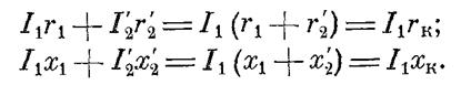
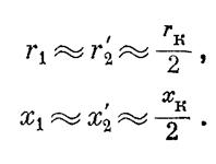
Resistance
and also z K are called active, inductive and impedances short circuit transformer, or short-circuit parameters of the transformer.
Then the equivalent circuit of the transformer is simplified even more. It will consist of two resistances r to and x k, through which the current I flows 1 (fig. 96, a).
The vector diagram corresponding to this equivalent circuit is shown in Figure 96, b. Usually
The setting of a passive smoothing filter at the output of the rectifier significantly affects the physical processes in the rectifier itself. An inductive character occurs when the rectifier operates on a filter, starting with inductance or on a relay winding, a contactor, an excitation winding of electrical machines, etc. The diagram of a simple rectifier with an inductive load is shown in Fig. 3.34. In these schemes, as a rule, the condition >> is satisfied, i.e. the inductive reactance of the choke at the ripple frequency is greater than the load resistance. It is known that the current in the inductance lags behind the voltage by π / 2 and the process of current rise and fall ends within one period.
Figure 3.34 - Single-phase, single-ended rectifier with
inductive nature of the load
The current in the circuit (i 2) is non-sinusoidal, since in addition to the EMF of the secondary winding, the induction EMF of the inductor operates in it.
When the current increases, energy is accumulated in the magnetic field of the inductor, and when the current decreases, this energy is released.
Thus, the result of switching on the inductance is the “pull-in” of the valve current. The angle of current flow depends on the time constant, where R = R N + r D + r 2, r D is the resistance of the diode, r 2 is the ohmic resistance of the secondary winding of the transformer (Figure 3.35).
Figure 3.35 - Dependence of the angle of current flow on the time constant
It is difficult to fulfill the ratio because the losses in the choke itself increase and the overall efficiency decreases significantly. Therefore, with an inductive nature of the load, polyphase circuits p ≥ 2 are used, where the continuity of the current is easily ensured during the ripple period.
Take a three-phase single-ended rectifier (Figure 3.36). In this figure, L S is the leakage inductance of the secondary winding; r - loss resistance (r = r 2 + r 1 / n 2), which is usually r<< Rн; – угол перекрытия фаз. Поскольку >> the current in the load is constant, and the current through the valve has the form rectangular pulse... The current transfer from valve to valve due to leakage inductance cannot occur instantaneously. Its EMF of self-induction prevents a change in current - in one phase it decreases, and in the other it increases. As a result, the current flows simultaneously in two phases. This phenomenon is called phase overlap. It significantly affects the qualitative and quantitative relationships in the rectification circuit.
Figure 3.36 - Three-phase single-ended rectifier
In a single-ended single-phase circuit, there is no current transition from one valve to another, therefore Ls in it practically does not affect physical processes. In a three-phase circuit, there is a finite current transition time (phase switching). If we neglect the resistance of the valves and the transformer, then there will be no pulling in of the current - the switching is instantaneous. Due to the phase overlap, the constant component U 0 decreases by the value of the triangle area in the voltage U d.
As a result, the presence of r and Ls leads to a sharper drop in the external characteristics of the rectifier (i.e. an increase in Rout), which is shown in Figure 3.37.
Figure 3.37 - External characteristic of a rectifier with an inductive
the nature of the load
Here, when the load current is less than a certain value I 0cr, the ratio ceases to be fulfilled. The choke current becomes intermittent, it discharges completely and the voltage rises.
For rectifiers with an inductive load, the following conclusions can be drawn:
1) The inductive component of resistance and load must be commensurate with Rн (otherwise the efficiency will be low).
2) The shape of the valve current curve is close to rectangular.
3) The duration of operation of each phase does not depend on the inductance in the load circuit, but is determined by the number of rectification phases (pulse rate) and the leakage inductance of the transformer.
4) The presence of leakage inductance leads to overlap of the phase currents, while U 0 decreases, and the ripple at the input of the smoothing filter increases.
Bridge nature of the load
The capacitive nature of the load occurs when the rectifier operates on a filter starting with a capacitance, as shown in Figure 3.38.
The constant of the charge circuit is much less than the constant of the discharge circuit, therefore the charge time (angle) is much less than the discharge time of the filter capacitor to the load. The valve current is cut off. With an increase in R H, the discharge slows down and the point of intersection of U 2 and U C shifts, the angle decreases, the voltage ripple also decreases. At current
Figure 3.38 - The simplest rectifier with a capacitive load
load equal to zero, the capacitor is not discharged and U 0 = U m 2. The reverse voltage across the valve is also maximum and equal. The external characteristic is non-linear and the output impedance can only be determined at the operating point through increments (Figure 3.39).
Figure 3.39 - External characteristic of a rectifier with a capacitive
load
The single-phase single-ended rectification circuit has rather high ripple at a low fundamental frequency and the transformer is poorly used. However, the simplicity of single-ended circuits makes them more attractive over push-pull circuits for obtaining high voltages.
Consider a voltage doubling circuit. It is shown in Fig. 3.40 and consists of two single-ended rectifiers, each of which uses its own
Figure 3.40 - Voltage doubling circuit (symmetrical)
half-wave of the mains voltage. The voltage across the load is the sum of the voltages across the capacitors C 1 and C 2. If the ripple is small, then the constant component at the load
The addition compensates for all odd harmonics, including the first one (p = 2). The disadvantage of the circuit is the lack of a common point between the transformer and the load, which is inconvenient from the point of view of electrical safety.
Another doubling scheme is shown in Figure 3.41. It is called unbalanced and has a common point of network and load.
Figure 3.41 - Unbalanced voltage doubling circuit
In this circuit, the frequency of the first harmonic of the ripple is equal to the mains frequency. Capacitor C1 performs the function of an intermediate energy storage device, therefore the mass and volume of an asymmetric doubler is greater than that of a symmetric one.
But the result is a regular structure that can be increased, as shown in Figure 3.42.
Figure 3.42 - Asymmetric voltage doubling circuit (a) and
voltage multiplier by six (b)
In the voltage multiplier, the load can also be connected to the upper group of capacitors - we get a multiplier by five. The multipliers are produced as a non-separable block. The number of capacitors is equal to the multiplication factor. The output impedance is measured in kilo-ohms.
Controlled rectifiers
A controlled rectifier is called a rectifier, in which, with a constant input voltage, the output voltage can be adjusted.
The output voltage can be controlled by switching the turns of the primary or secondary windings of the transformer, by a laboratory autotransformer (LATR) or by introducing a rheostat into the current circuit. The first method provides discreteness of regulation, which is not always acceptable, the second one has low reliability due to the presence of sliding contacts, and the third (using rheostats) has low efficiency. Therefore, controlled valves are used, which are included instead of uncontrolled ones in the rectification circuit.
Thyristors are used as such valves - four-layer p-n-p-n structures... Figure 3.43a, b, c shows the conventional designation, equivalent circuit and CVC of the thyristor (triac), respectively. :
Figure 3.43 - Symbol, equivalent circuit and CVC of the thyristor
In the normal state, the thyristor is locked. There are two stable states in the scheme: open (point A) and closed (point B).
An increase in the source voltage from 0 to E at Iue = 0 leads to a displacement of the operating point along the lower section of the characteristic. If we apply a pulse of the control current Iue sufficient for switching on, then the r.t. will go to point A and the control circuit will cease to affect the processes in the anode circuit of the thyristor - the control circuit is not needed. This is a system with an inner positive feedback Therefore, thyristors have a high power gain.
Usually E is always less than the anode switch-on voltage (U amax) by 20 ... 30%. It is possible to turn off the thyristor only by decreasing Ia to a level less than the holding current (Isp), by increasing Rn or decreasing E.
V open state thyristors transmit large currents (hundreds of amperes), but they are inertial, the turn-on time is 0.1 ... 10 μs, and the turn-off time is 1 ... 100 μs.
Along with the considered thyristor, there is a group of four-layer devices with various properties, these are dinistors, triacs and lockable thyristors. They are shown in Fig. 3.44.
Figure 3.44 - Conventional designation of dinistor (a), triac (b)
and a lockable thyristor (c).
The dinistor has a regulated turn-on voltage across the anode. This is a two-electrode device. The triac is designed to operate in alternating current circuits, while the control signal can be applied relative to the cathode or relative to the anode. All of the above devices are turned off only by reducing its anode current below the holding current.
However, there are also so-called lockable thyristors, i.e. by supplying current to the UE circuit of the reverse direction, the thyristor can be turned off. But at the same time, the turn-off gain is an order of magnitude lower than the turn-on gain.
All of these devices are widely used in automation devices and power supplies as regulators, stabilizers and protection devices.
Typically, a thyristor is placed in a rectifier circuit instead of an uncontrolled valve. Take a single-phase bridge (Figure 3.45). In this figure - the angle of the thyristor switching on (the angle relative to the point of natural switching on of the uncontrolled valve).
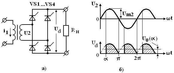
Figure 3.45 - Single-phase controlled bridge
Let's find the constant component of the voltage across the load.
Considering that the voltage U 2 is harmonic, then
(3.44) If we accept in (3.44), then is the voltage at the output of the uncontrolled rectifier; if, then. The dependence is the control characteristic of the controlled rectifier. It is shown in Figure 3.46 and is non-linear.
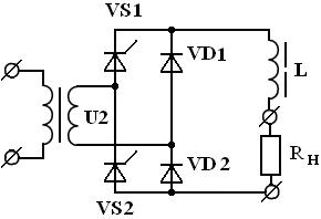
Figure 3.49 - Asymmetrical controlled rectifier
Here, the diodes play the role of a zero gate, therefore; asymmetry can be any (uncontrolled valves can be in the anode or cathode group, or as in Figure 3.49).
Thyristors are also used in booster circuits, which, in comparison with the considered ones, have a higher efficiency, since they convert only part of the energy for the load. The rectifier circuit with voltage boost is shown in Fig. 3.50. Here is the minimum output voltage
Figure 3.50 - Rectifier with voltage boost
provided by the uncontrolled rectifier VD1 and VD2. The increase in voltage is achieved by turning on the thyristors VS1 and VS2. In the maximum mode, the diodes are always closed and the switching angle. Such circuits have good energy performance, but additional windings on the transformer are required.
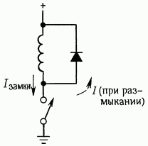
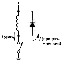
What happens if you open the inductor current control switch? Inductance, as you know, is characterized by the following property: and from this it follows that the current cannot be turned off instantly, since in this case an infinite voltage would appear on the inductance. In fact, the voltage across the inductor rises sharply and continues to rise until a current appears. Electronic devices that drive inductive loads may not be able to withstand this voltage rise, especially for components that undergo "breakdown" at some voltage values. Consider the circuit shown in Fig. 1.94.

Rice. 1.94. Inductive "throw".
In the initial state, the switch is closed and a current flows through the inductance (which can be, for example, the relay winding). When the switch is open, the inductance "tends" to provide current between points A and B, flowing in the same direction as when the switch is closed. This means that the potential of point B becomes more positive than the potential of point A. In our case, the potential difference can reach 1000 V before an electric arc occurs in the switch, which closes the circuit. This shortens the life of the switch and generates impulse pickups that can affect the operation of nearby circuits. If you imagine that a transistor is used as a switch, then the life of such a switch is not shortened, but simply becomes zero!
To avoid such troubles, it is best to connect a diode to the inductor, as shown in Fig. 1.95. When the switch is closed, the diode is reverse biased (due to voltage drop direct current on the winding of the inductor). When the switch is opened, the diode opens and the potential of the switch contact becomes higher than the potential of the positive supply voltage by the amount of voltage drop across the diode. The diode must be sized to withstand an initial current equal to the steady state current through the inductor; suitable for example diode type.
Rice. 1.95. Blocking inductive throw.
The only drawback of the described circuit is that it delays the decay of the current flowing through the coil, since the rate of change of this current is proportional to the voltage across the inductor. In cases where the current must decay quickly (for example, high-speed contact printers, high-speed relays, etc.), the best result can be obtained if a resistor is connected to the inductor coil, choosing it so that the value does not exceed the maximum allowable voltage for switch. (The fastest decay for a given maximum voltage can be obtained by connecting a zener diode to the inductor, which provides a linear rather than exponential decay.)
Diode protection cannot be used for AC circuits containing inductors (transformers, AC relays), as the diode will be open during the half-cycles of the signal when the switch is closed. In such cases, it is recommended to use the so-called RC-damping chain (Fig. 1.96). The R and C values shown in the diagram are typical for small inductive loads connected to AC power lines. A damper of this type should be provided in all devices operating on voltages of AC power lines, since the transformer is an inductive load. An element such as a metal oxide varistor can also be used for protection.
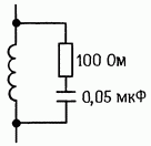
Rice. 1.96. RC "damper" for suppressing inductive surge.
It is an inexpensive item that is similar in appearance on a ceramic capacitor, and on electrical characteristics to a bi-directional zener diode. It can be used in a voltage range of 10 to 1000 V for currents up to thousands of amperes (see Section 6.11 and Table 6.2). Connecting a varistor to the external terminals of the circuit allows not only to prevent inductive pickups to nearby devices, but also to suppress large signal spikes that sometimes occur in the power line and pose a serious threat to equipment.
What happens if you open the inductor current control switch? Inductance, as you know, is characterized by the following property: U = L (dI / dt), and from this it follows that the current cannot be turned off instantly, since in this case an infinite voltage would appear on the inductance. In fact, the voltage across the inductor rises sharply and continues to rise until a current appears. Electronic devices that drive inductive loads may not be able to withstand this voltage surge, especially in components that experience "breakdown" at some voltage levels. Consider the circuit presented
Rice. 1.94. Inductive "throw".
in fig. 1.94. In the initial state, the switch is closed and a current flows through the inductance (which can be, for example, the relay winding). When the switch is open, the inductance "tends" to provide current between points A and B, flowing in the same direction as when the switch is closed. This means that the potential of point B becomes more positive than the potential of point A. In our case, the potential difference can reach 1000 V before an electric arc occurs in the switch, which closes the circuit. This shortens the life of the switch and generates impulse pickups that can affect the operation of nearby circuits. If you imagine that a transistor is used as a switch, then the life of such a switch is not shortened, but simply becomes zero!
To avoid such troubles, it is best to connect a diode to the inductor, as shown in Fig. 1.95. When the switch is closed, the diode is reverse biased (due to the DC voltage drop across the inductor winding). When the switch is opened, the diode opens and the potential of the switch contact becomes higher than the potential of the positive supply voltage by the amount of voltage drop across the diode. The diode must be sized to withstand an initial current equal to the steady state current through the inductor; suitable, for example, a diode type 1N4004.
Rice. 1.95. Blocking inductive throw.
The only drawback of the described circuit is that it delays the decay of the current flowing through the coil, since the rate of change of this current is proportional to the voltage across the inductor. In cases where the current must decay quickly (for example, high-speed contact printers, high-speed relays, etc.), the best result can be obtained if a resistor is connected to the inductor, choosing it so that the value of U and + IR does not exceed the maximum allowable voltage on the switch. (The fastest decay for a given maximum voltage can be obtained by connecting a zener diode to the inductor, which provides a linear rather than exponential decay.)
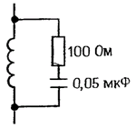
Figure 1.96. RC - "damper" for suppressing inductive surge.
Diode protection cannot be used for AC circuits containing inductors (transformers, AC relays), as the diode will be open during the half-cycles of the signal when the switch is closed. In such cases, it is recommended to use the so-called RC-damping chain (Fig. 1.96). The R and C values shown in the diagram are typical for small inductive loads connected to AC power lines. A damper of this type should be provided in all devices operating on voltages of AC power lines, since the transformer is an inductive load. An element such as a metal oxide varistor can also be used for protection. It is an inexpensive element, similar in appearance to a ceramic capacitor, and in electrical characteristics to a bidirectional zener diode. It can be used in a voltage range of 10 to 1000 V for currents up to thousands of amperes (see.