It would seem that it couldn’t be easier, I turned on the power and the device containing the MK started working. However, in practice there are cases when a conventional mechanical toggle switch is not suitable for these purposes. Illustrative examples:
- the microswitch fits well into the design, but it is designed for low switching current, and the device consumes an order of magnitude more;
- it is necessary to remotely turn on/off the power using a logical level signal;
- The power switch is made in the form of a touch (quasi-touch) button;
- It is required to perform a “trigger” power on/off by repeatedly pressing the same button.
For such purposes, special circuit solutions, based on the use of electronic transistor switches (Fig. 6.23, a...m).
Rice. 6.23. Electronic power supply circuits (beginning):
a) SI is a “secret” switch used to restrict unauthorized access to a computer. Low-power toggle switch opens/closes field-effect transistor VT1, which supplies power to the device containing the MK. When the input voltage is higher than +5.25 V, it is necessary to install an additional stabilizer in front of the MK;
b) turning on/off the +4.9 V power supply with a digital ON-OFF signal through the DDI logic element and switching transistor VT1
c) low-power “quasi-touch” button SB1 triggers on/off the +3 V power supply through the DDL chip. Capacitor C1 reduces contact “bounce.” LED HL1 indicates current flow through key transistor VTL The advantage of the circuit is its very low self-current consumption in the off state;

Rice. 6.23. Electronic power supply circuits (continued):
d) supply voltage +4.8 V with a low-power SBI button (without self-reset). The +5 V input power supply must have current protection so that the VTI transistor does not fail if there is a short circuit in the load;
e) switching on the +4.6 V voltage using an external signal £/in. Galvanic isolation is provided on the optocoupler VU1. The resistance of the resistor RI depends on the amplitude £/in;
e) buttons SBI, SB2 must be self-returning, they are pressed in turn. The initial current passing through the contacts of the SB2 button is equal to the total load current in the +5 V circuit;
g) L. Coyle’s diagram. The VTI transistor automatically opens when the XP1 plug is connected to the XS1 socket (due to resistors R1, R3 connected in series). At the same time, a sound signal from the audio amplifier is supplied to the main device through elements C2, R4. The RI resistor may not be installed if the active resistance of the “Audio” channel is low;
h) similar to Fig. 6.23, v, but with a switch on the field-effect transistor VT1. This allows you to reduce your own current consumption both in the off and on states;

Rice. 6.23. Electronic power supply circuits (end):
i) scheme for activating MK for a strictly fixed period of time. When the contacts of switch S1 are closed, capacitor C5 begins to charge through resistor R2, transistor VTI opens, and the MK turns on. As soon as the voltage at the gate of transistor VT1 decreases to the cutoff threshold, the MK turns off. To turn it on again, you need to open contacts 57, wait a short pause (depending on R, C5) and then close them again;
j) galvanically isolated switching on/off the +4.9 V power supply using signals from the COM port of the computer. Resistor R3 maintains the closed state of transistor VT1 when the optocoupler VUI is “off”;
l) remote on/off integral stabilizer voltage DA 1 (Maxim Integrated Products) through the COM port of the computer. The +9 V supply can be reduced down to +5.5 V, but in this case it is necessary to increase the resistance of resistor R2 so that the voltage at pin 1 of the DA I chip becomes greater than at pin 4;
l) voltage stabilizer DA1 (Micrel) has a power-on input EN, which is controlled by a HIGH logic level. The RI resistor is needed so that pin 1 of the DAI chip does not “hang in the air,” for example, in the Z-state of the CMOS chip or when the connector is unplugged.
The corridor switch is very familiar to older generation electricians. Nowadays such a device is somewhat forgotten, so we will have to briefly talk about the algorithm of its operation.
Imagine that you are leaving a room into a corridor that has no windows. You flip the switch near the door, and the light comes on in the corridor. Let's call this switch the first one.
Having reached the opposite end of the corridor, before going out into the street, you turn off the light with the second switch located near the exit door. If there is still someone left in the room, then when leaving, he can also turn on the light with the first switch, and turn it off with the second. When entering the corridor from the street, the light is turned on by the second switch, and in the room it is turned off by the first.
Although the entire device is called a switch, it requires two changeover switches to make one. Ordinary switches will not work here. The diagram of such a corridor switch is shown in Figure 1.
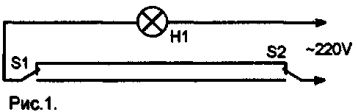
Figure 1. Corridor switch with two switches.
As can be seen from the figure, the circuit is quite simple. The light will light if both switches S1 and S2 are connected to the same wire, either upper or lower, as shown in the diagram. Otherwise the lamp is extinguished.
To control one light source from three places, not necessarily one light bulb, it can be several lamps under the ceiling, the circuit is different. It is shown in Figure 2.
Figure 2. Corridor switch with three switches.
Compared to the first scheme, this scheme is somewhat more complicated. A new element has appeared in it - switch S3, which contains two groups of switching contacts. In the position of the contacts indicated in the diagram, the lamp is on, although the position in which the consumer is off is usually indicated. But with this outline, it is easier to trace the path of the current through the switches. If now any of them is moved to the position opposite to that indicated in the diagram, the lamp will turn off.
To trace the current path for other switch positions, simply move your finger along the diagram and mentally move them to all possible positions.
Usually this method allows you to deal with more complex circuits. Therefore, a long and boring description of the operation of the circuit is not given here.
This scheme allows you to control lighting from three places. It can find application in a corridor into which two doors open. Of course, one could argue that in this case it is easier to install a modern motion sensor, which even monitors whether it is day or night. Therefore, the lighting will not turn on during the day. But in some cases, such automation simply will not help.
Imagine that such a triple switch is installed in a room. One key is located at front door, the other one is above desk, and the third is near the bed. After all, automation can turn on the lights when you are just in you'll roll over in your sleep from side to side. You can find many more conditions where a circuit without automation is needed. These switches are also called passable, and not just bellhops.
Theoretically such pass-through switch It can be done with a large number of switches, but this will significantly complicate the circuit; switches with more and more contact groups will be required. Even just five switches will make the circuit inconvenient for installation and simply understanding the principles of its operation.
What if such a switch is needed for a corridor into which ten or even twenty rooms open? The situation is quite real. There are enough such corridors in provincial hotels, student and factory dormitories. What to do in this case?
This is where electronics come to the rescue. After all How does a pass-through switch work? When you press one key, the light turns on and stays on until you press another. This algorithm of work resembles the work electronic device- trigger. You can read more about various triggers in the series of articles “”.
If you just stand and press the same key, the light will turn on and off alternately. This mode is similar to the operation of a trigger in the counting mode - with the arrival of each control pulse, the state of the trigger changes to the opposite.
In this case, first of all, you should pay attention to the fact that when using a trigger, the keys should not be fixed: just buttons, like bell buttons, are enough. To connect such a button you only need two wires, and not even very thick ones.
And if you connect another one in parallel with one button, you get a pass-through switch with two buttons. Without changing anything in schematic diagram, you can connect five, ten or more buttons. The circuit using the K561TM2 trigger is shown in Figure 3.

Figure 3. Pass-through switch on the K561TM2 trigger.
The trigger is enabled in counting mode. To do this, its inverse output is connected to input D. This is a standard connection, in which each input pulse at input C changes the trigger state to the opposite.
Input pulses are obtained by pressing the S1…Sn buttons. The R2C2 chain is designed to suppress contact bounce and form a single pulse. When you press the button, capacitor C2 is charged. When the button is released, the capacitor is discharged through the C - input of the trigger, forming an input pulse. This ensures smooth operation of the entire switch.
The R1C1 chain connected to the R input of the flip-flop provides a reset when the power is initially turned on. If this reset is not required, then the R - input should simply be connected to the common power wire. If you leave it just “in the air”, then the trigger will perceive this as a high level and will be in the zero state all the time. Since the RS inputs of the trigger are priority, the supply of pulses to input C will not be able to change the state of the trigger, the entire circuit will be inhibited and inoperable.
An output stage that controls the load is connected to the direct output of the trigger. The simplest and reliable option these are a relay and a transistor as shown in the diagram. A diode D1 is connected in parallel to the relay coil, the purpose of which is to protect the output transistor from self-induction voltage when relay Rel1 is turned off.
The K561TM2 chip in one package contains two triggers, one of which is not used. Therefore, the input contacts of an unused trigger should be connected to a common wire. These are pins 8, 9, 10 and 11. This connection will prevent the microcircuit from failing due to static electricity. For CMOS microcircuits, such a connection is always required. The +12V supply voltage should be applied to pin 14 of the microcircuit, and pin 7 should be connected to the common power wire.
As transistor VT1, you can use KT815G, diode D1 type 1N4007. The relay is small-sized with a 12V coil. The operating current of the contacts is selected depending on the power of the lamp, although there may be any other load. Here it is best to use imported relays such as TIANBO or the like.
The power supply is shown in Figure 4.
Figure 4. Power supply.
The power supply is made according to a transformer circuit using an integrated stabilizer 7812, providing a constant voltage of 12V at the output. A transformer with a power of no more than 5...10 W with a secondary winding voltage of 14...17V is used as a network transformer. Diode bridge Br1 can be used like KTs407, or assembled from 1N4007 diodes, which are currently very common.
Imported electrolytic capacitors such as JAMICON or similar. They are now also easier to buy than parts domestic production. Although the 7812 stabilizer has built-in protection against short circuits, but you should still make sure that the installation is correct before turning on the device. This rule should never be forgotten.
The power source, made according to the specified circuit, provides galvanic isolation from the lighting network, which allows this device to be used in damp rooms, such as cellars and basements. If there is no such requirement, then the power source can be assembled using a transformerless circuit, similar to the one shown in Figure 5.
Figure 5. Transformerless power supply.
This scheme allows you to abandon the use of a transformer, which in some cases is quite convenient and practical. True, the buttons, and the entire structure as a whole, will have a galvanic connection with lighting network. You should not forget about this and follow safety rules.
The rectified mains voltage is supplied through ballast resistor R3 to the zener diode VD1 and is limited at 12V. Voltage ripples are smoothed out by electrolytic capacitor C1. The load is turned on by transistor VT1. In this case, resistor R4 is connected to the direct output of the trigger (pin 1), as shown in Figure 3.
The circuit, assembled from serviceable parts, does not require adjustment and starts working immediately.
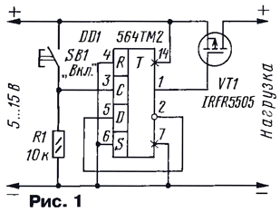
This device allows you to turn the load on and off by pressing one button without locking. It is based on a T-trigger formed by a D-trigger and a single-shot input to eliminate contact bounce and interference. Using the device, you can control, for example, turning on the light. The control input reacts to a short to ground, which also allows the device to be used in a car.
Principle of operation
The circuit contains 2 D flip-flops. The first one is connected according to a one-shot circuit. Inputs D and CLK are shorted to common, and they always have a logical zero. Through R2, a logical one is supplied to input S. The output is connected to the RESET pin via an RC circuit. Next comes standard scheme T-flip-flop based on D-flip-flop - the D input is connected to the inverting output, and the RS pins are not used and are connected to common.
Let's see what happens when you press the button.
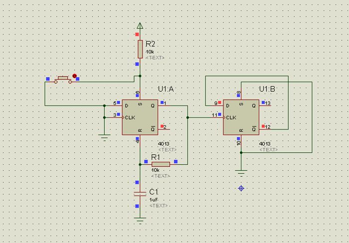
At the moment the button is pressed, a logical zero arrives at pin S, it also goes to the output, and through R1 it resets the trigger, which goes to the initial state. Capacitor C1 smoothes the cycle, and its capacitance determines how long the button must be pressed for the trigger to work.
After pressing the button, the device status becomes as follows:

The only change compared to the initial state is that the trigger output has acquired a logical one state. It will maintain this state until the next press, then the output will go back to the logic zero state.
Schematic diagram
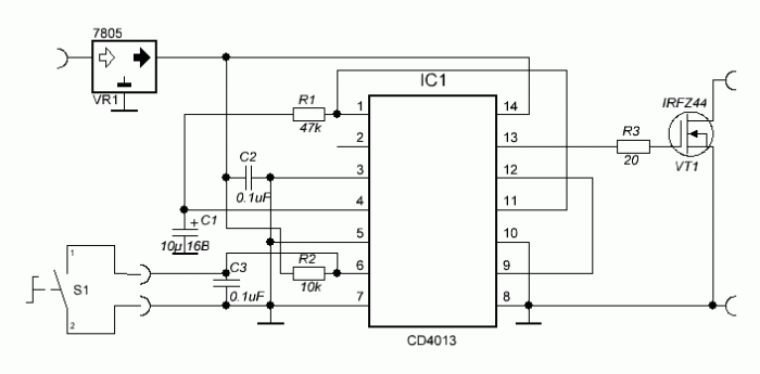
To switch the load, the trigger controls the field-effect transistor VT1 through the current-limiting resistor R3. Power supply for the circuit is 7-35V.
The device assembled on a breadboard looks like this:

List of radioelements
| Designation | Type | Denomination | Quantity | Note | Shop | My notepad |
|---|---|---|---|---|---|---|
| VR1 | Linear regulator | LM7805CT | 1 | Search in LCSC | To notepad | |
| IC1 | Trigger | CD4013B | 1 | Search in LCSC | To notepad | |
| VT1 | MOSFET transistor | IRFZ44R | 1 | Search in LCSC | To notepad | |
| R1 | Resistor | 47 kOhm | 1 | Search in LCSC | To notepad | |
| R2 | Resistor | 10 kOhm | 1 | Search in LCSC | To notepad | |
| R3 | Resistor | 20 ohm | 1 | Search in LCSC | To notepad | |
| C1 | Electrolytic capacitor | 10uF 16V | 1 |
Almost every radio amateur has at least once used P2K switches, which can be single (with or without latching) or assembled in groups (without latching, independent latching, dependent latching). In some cases, it is more expedient to replace such switches with electronic ones assembled on TTL microcircuits. It is these switches that we will talk about.
Latching switch. The equivalent in digital circuitry of such a switch is a flip-flop with a counting input. When you press the button for the first time, the trigger goes into one stable state, and when you press it again, it goes into the opposite state. But it is impossible to directly control the counting input of the trigger with a button due to the bounce of its contacts at the moment of closing and opening. One of the most common methods of combating bounce is to use a switch button in conjunction with a static trigger. Let's take a look at Fig. 1.
Fig.1
In the initial state, the outputs of elements DD1.1 and DD1.2 are “1” and “0”, respectively. When you press the SB1 button, the very first closure of its normally open contacts switches the trigger assembled on DD1.1 and DD1.2, and contact bounce does not affect its further fate - in order for the trigger to return to its original state, it is necessary to apply a logical zero to its lower element . This can only happen when the button is released and again the chatter will not affect the reliability of the switching. Next, our static trigger controls a regular counter, which is switched by input C with the edge of the signal from output DD1.2.
The following circuit (Fig. 2) works similarly, but allows you to save one case, since the second half of the DD1 chip is used as a static trigger.
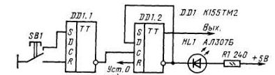
Fig.2
If the use of buttons with switching contacts is inconvenient, then you can use the diagram shown in Fig. 3.
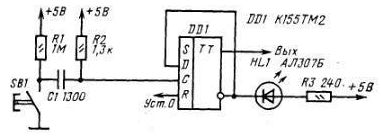
Fig.3
It uses the R1, C1, R2 chain as a bounce suppressor. In the initial state, the capacitor is connected to the +5 V circuit and is discharged. When you press the SB1 button, the capacitor starts charging. As soon as it charges, a negative pulse will be generated at the input of the counting trigger, which will switch it. Since the charging time of the capacitor is much longer than the time of transient processes in the button and is about 300 ns, the bouncing of the button contacts does not affect the state of the trigger
Latching and Master Reset Switches. The circuit shown in Fig. 4 represents an arbitrary number of buttons with independent fixation and one general reset button.

Fig.4
Each switch is a static trigger, activated by a separate button. Since when even a short low level appears, the trigger unambiguously switches and is held in this position until the “reset” signal at the other input, a debouncing circuit for the button contacts is not needed. The reset inputs of all flip-flops are connected and connected to the SBL button, which is a common reset button. Thus, you can turn on each trigger with a separate button, but you can only turn it off all at once with the “Reset” button.
Latent Switches. In this scheme, each button turns on its static trigger and simultaneously resets all others. Thus, we get an analogue of the line of P2K buttons with dependent fixation (Fig. 5).

Fig.5
As in the previous circuit, each button turns on its own trigger, but at the same time it starts a reset circuit assembled on transistor VT2 and elements DK.3, DK.4. Let's consider the operation of this node. Suppose we need to enable the first trigger (elements D1.1, D1.2). When you press the SB1 button, a low level (since capacitor C1 is discharged) will switch the trigger (input of element D1.1). The capacitor will immediately begin to charge through the circuit SB1, R8. As soon as the voltage on it increases to approximately 0.7V, transistor VT1 opens, but for element D1.1 this voltage is still logical “0”.
The transistor will immediately switch the Schmidt trigger on elements DK.3, DK.4, which will generate a short pulse at the reset inputs of all triggers. All triggers will be reset (if they were turned on before), except for the first one, since logical “0” (voltage below 1 V) is still supplied to its upper input in the circuit through the SB1 button. Thus, the delay in the passage of the reset signal is sufficient to stop the contact bounce, but the reset will occur faster than we release the button that prohibits switching the corresponding trigger
An interesting and simple switch circuit with dependent latching can be built on the K155TM8 microcircuit (Fig. 6).

Fig.6
When power is applied, the R6, C1 chain resets all flip-flops and their direct outputs are set to a low logic level. At inputs D the level is also low, since they are all connected through their own button to the common wire. Let's assume the SB1 button is pressed. The input of the first trigger is set to “1” (thanks to R1), and the general clock input is set to “0” (via the switching contact of the button). So far, theoretically, nothing happens, since the microcircuit gates the data on a positive edge. But when the button is released, the data from the inputs will be copied into flip-flops - into 2, 3, 4 - “0”, into 1 - “1”, since the positive edge at input C appears before the upper contacts SB1 in the circuit are closed. When any other button is pressed, the cycle will repeat, but “1” will be written to the trigger whose button is pressed. This is in theory. In practice, due to contact bounce, the data from the input will be overwritten immediately after pressing the button and will not change when it is released.
All of the above schemes with dependent latching have one significant drawback, which is also characteristic of P2K switches - the ability to “snap” several buttons when they are pressed simultaneously. A circuit assembled on a priority encoder will allow you to avoid this (Fig. 7).
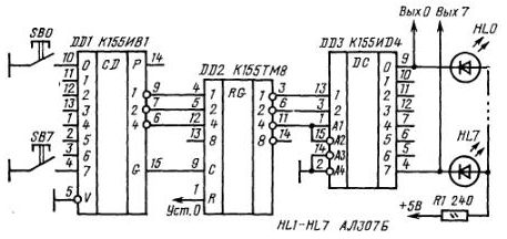
Fig.7
The circuit, of course, looks quite cumbersome, but in fact it consists of only three buildings without additional attachments and, importantly, does not require switching buttons. When you press the button, the priority encoder DD1 sets the binary code (inverse) of this button at its output and confirms it with the G “strobe” signal, which immediately writes data to the DD2 chip, operating in the mode of a four-bit parallel latch register. Here the code is inverted again (the outputs of the register are inverted) and goes to the usual binary decimal decoder DD3. Thus, the corresponding output of the decoder is set to a low level, which will remain unchanged until any other button is pressed. The impossibility of latching two buttons simultaneously is ensured by the priority circuit (I wrote more about the operation of the priority encoder). Since the K155IV1 microcircuit was designed to increase the bit capacity, it would be stupid not to take advantage of this and assemble a block of radio-latching switches for 16 buttons (Fig. 8).

Fig.8
I will not dwell on the operation of the circuit, since I have described in detail the principle of increasing the capacity of IV1. The pinout of the TTL power pins of the K155 series microcircuits (1533, 555, 133) can be seen.
Currently, electronic switches are often used in electronic equipment, in which one button can be used to turn it on and off. You can make such a switch powerful, economical and small-sized by using a field-effect switching transistor and a digital CMOS chip.
A diagram of a simple switch is shown in Fig. 1. Transistor VT1 performs the functions of an electronic key, and trigger DD1 controls it. The device is constantly connected to a power source and consumes a small current - units or tens of microamps.
If the direct output of the trigger is at a high logical level, then the transistor is closed and the load is de-energized. When the contacts of the SB1 button are closed, the trigger will switch to the opposite state, and a low logic level will appear at its output. Transistor VT1 will open and voltage will be supplied to the load. The device will remain in this state until the button contacts are closed again. Then the transistor will close, the load will be de-energized.
The transistor indicated in the diagram has a channel resistance of 0.11 Ohm, and the maximum drain current can reach 18 A. It should be taken into account that the gate-drain voltage at which the transistor opens is 4...4.5 V. At a supply voltage of 5. ..7 V The load current should not exceed 5 A, otherwise the voltage drop across the transistor may exceed 1 V. If the supply voltage is higher, the load current can reach 10... 12 A.
When the load current does not exceed 4 A, the transistor can be used without a heat sink. If the current is higher, a heat sink is necessary, or a transistor with lower channel resistance should be used. It is not difficult to select it from the reference table given in the article “Powerful switching transistors from International Rektifier” in “Radio”, 2001, No. 5, p. 45.
Such a switch can also be assigned other functions, for example, automatically switching off the load when the supply voltage drops or exceeds a preset value. In the first case, this may be necessary when powering the equipment from battery in order to prevent its excessive discharge, in the second - to protect the equipment from overvoltage.
The diagram of an electronic switch with a shutdown function when the voltage drops is shown in Fig. 2. It additionally contains a transistor VT2, a zener diode, a capacitor and resistors, one of which is adjusted (R4).
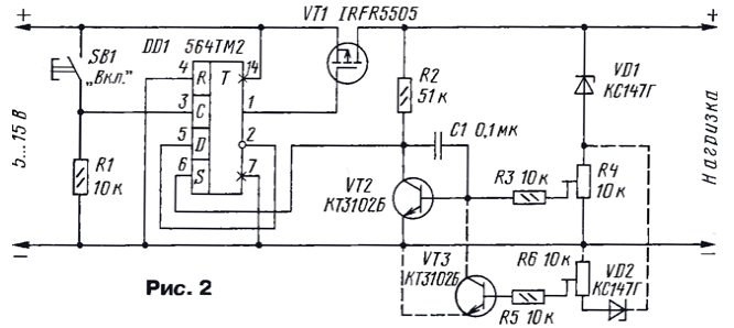
When you press the SB 1 button, the field-effect transistor VT1 opens, and voltage is supplied to the load. Due to the charging of capacitor C1, the voltage at the collector of the transistor at the initial moment will not exceed 0.7 V, i.e. will be logic low. If the voltage at the load becomes greater than the value set by the tuning resistor, a voltage sufficient to open it will be supplied to the base of the transistor. In this case, the “S” input of the trigger will remain at a low logical level, and the button can turn the power to the load on and off.
As soon as the voltage drops below the set value, the voltage on the trimmer resistor motor will become insufficient to open transistor VT2 - it will close. In this case, the voltage at the transistor collector will increase to a high logical level, which will go to the “S” input of the trigger. A high level will also appear at the output of the trigger, which will lead to the closing of the field-effect transistor. The load will be de-energized. Pressing the button in this case will only lead to a short-term connection of the load and its subsequent disconnection.
To introduce protection against excess supply voltage, the machine should be supplemented with transistor VT3, zener diode VD2 and resistors R5, R6. In this case, the device operates similarly to that described above, but when the voltage increases above a certain value, the transistor VT3 will open, which will lead to the closing of VT2, the appearance high level at the input "S" of the trigger and closing the field-effect transistor VT1.
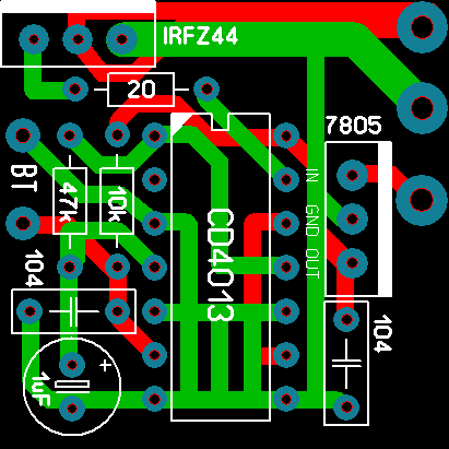
In addition to those indicated in the diagram, the device can use the K561TM2 microcircuit, bipolar transistors KT342A-KT342V, KT3102A-KT3102E, and a zener diode KS156G. Fixed resistors - MLT, S2-33, R1-4, tuned resistors - SPZ-3, SPZ-19, capacitor - K10 17, button - any small-sized one with self-resetting.
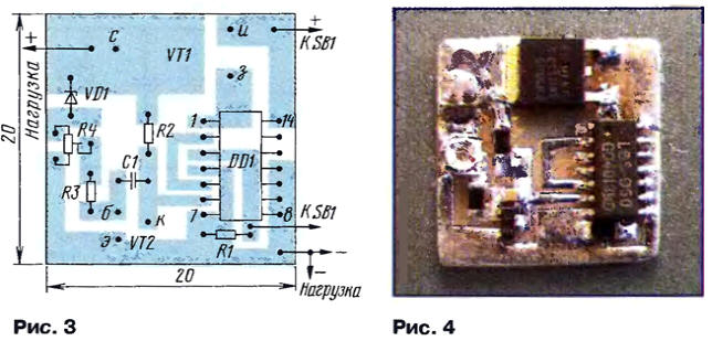
When using parts for surface mounting (chip CD4013, bipolar transistors KT3130A-9 - KT3130G-9, zener diode BZX84C4V7, fixed resistors P1-I2, capacitor K10-17v), they can be placed on a printed circuit board (Fig. 3) made of one-sided foil fiberglass with dimensions 20x20 mm. The appearance of the mounted board is shown in Fig. 4.