Transistor pulse and digital technology is based on the operation of the transistor as a key. Closing and opening the load circuit is the main purpose of a transistor operating in switching mode. By analogy with a mechanical switch (relay, contactor), the quality of a transistor switch is determined primarily by the voltage drop (residual voltage) across the transistor in the closed (open) state, as well as the residual current of the transistor in the off (closed) state.
The importance of considering the properties of a transistor switch for understanding the subsequent material follows from the fact that by changing the states of the transistor in a series circuit with a resistor and a power source, in essence, the formation of pulse-shaped signals, as well as various transformations, is carried out pulse signals in circuits and components of pulse technology. The transistor is also used as a contactless switch in DC and AC circuits to regulate the power supplied to the load.
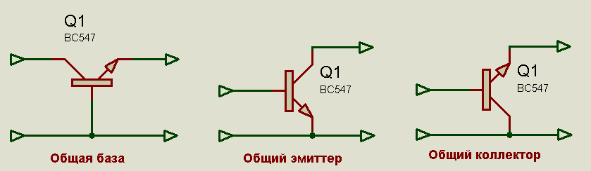
The basis of all units and circuits of pulsed and digital technology is the so-called key circuit - a cascade on a transistor operating in the key mode. The construction of the key circuit is similar to an amplifier stage. A transistor in a key circuit can be connected with a common base, a common emitter and a common collector. Most widespread received the OE diagram. This type of inclusion of a bipolar transistor is used further when considering the key mode of its operation.
Figure 4.3 - Key circuit on a transistor and graphical definition of the modes of the open and closed states of the transistor
Key circuit on transistor type p-p-p shown in Figure 4.3, A. Transistor T performs the function of a switch in a series circuit with a resistor R K and power source.
For the convenience of considering the processes in the circuit in the open and closed states of the transistor, we will use a graphic-analytical method based on constructing a load line a - b By DC(Figure 4.3, b).
The load line is described by the relation U ke = − ( E k − I To R j) and is carried out in the same way as for the amplifier stage. The intersection points of the load line with the current-voltage characteristics of the transistor determine the voltages on the elements and the current in the series circuit.
The blocking mode (cut-off mode) of the transistor is carried out by applying a voltage of positive polarity to its input ( U in > 0), indicated in Figure 4.3, A without parentheses. Under the influence of the input voltage, the emitter junction of the transistor is turned off ( U be > 0) and its current I e = 0. At the same time, through a resistor R b the reverse (thermal) current of the collector junction flows I k0 . The closed state of the transistor corresponds to the point M h (see Figure 4.3, b).
Thermal current flowing through the load I k0 is due to the fact that the transistor in the closed state does not ensure complete shutdown of the load resistor R to from the power source. Low value I k0 is one of the criteria for choosing a transistor for the key operating mode.
The value of the blocking input voltage U input z an is chosen so that when flowing through the resistor R b thermal current, the following conditions were met:
U bae= U input z an − I k0 R b > 0.
Voltage U 6e for germanium transistors is 0.5...2.0 V.
Mode open state transistor is achieved by changing the polarity of the input voltage ( U input< 0) и заданием соответствующего тока базы. Открытое состояние транзистора характеризует точка M o on the load line.
Let's define the necessary conditions to create an open state of the transistor. For this purpose, we assume that for U input< 0 ток базы I b increases gradually. An increase in the base current will correspond to an increase in the collector current and a movement of the operating point from the position M h up along the load line. Voltage U ke of the transistor gradually decreases. Up to a certain limit value of the base current I b.gr the known proportional relationship between I to and I b.
We covered the basics of amplifiers and talked a little about what feedback and gain are. A calculation of the operational amplifier circuit was given. Now we're ready to look a little deeper to understand the basics.
A transistor can be represented as a variable resistance. The position of the regulator depends on the current supplied to the base. If no current is supplied, the collector-emitter junction resistance is very high. When a small current is applied to the base, the resistance variable resistor will decrease and chains K-E a current will flow h21 times greater than the base current. H21 is the gain value of the transistor, found in the reference book.
If the base current is gradually increased, the junction resistance will gradually decrease until it becomes close to zero. At this moment, the transistor will be completely open; it is this mode that we considered in the article about connecting a load using a transistor.
This time we are interested in the intermediate state, since the input and output are interconnected, the output signal will be a copy of the input, but amplified several times. Now let's look at the gain. The fact is that h21 has a fairly large spread for one type of transistor, it can range from 400 to 1000. It also depends on temperature. Therefore, there is typical diagram gain, which takes into account all these shortcomings. But for general development It’s worth telling what they generally are.
Let us remember that we imagined the amplifier as a black box - two input legs and two output legs. In the case of a transistor, one of the legs will always be common for the input and output. Depending on this, the transistor can be connected according to a circuit with a common base, a common collector and a common emitter.
Each of these schemes has its own advantages and disadvantages. Our goal is to consider the connection using a common emitter circuit, because this circuit allows you to amplify both current and voltage.
In fact, there is a lot of information on calculating a common emitter circuit on the Internet, but in my opinion, it is not suitable for a person who has difficulty imagining what a transistor looks like. Here we will consider the most simplified version, which will allow us to obtain a very approximate, but, in my opinion, understandable result. Therefore, we will try to sort everything out step by step.
A real transistor has several features that must be taken into account when designing the circuit. For example, if a small amplitude signal is applied to the base, then nothing will happen at the output - the transistor simply will not open. In order for a signal to appear at the output, it must be opened slightly, i.e. apply a bias voltage of about 0.7V to the base. Typically this voltage is supplied using a voltage divider. We don’t pay attention to the resistor values for now; the calculation will be a little further.

The next moment, when the transistor opens, current will flow through the collector-emitter circuit, and when the transistor is fully open, the current will be limited only by the power source. Therefore, the transistor may burn out. The maximum current value is given in the reference book, therefore, to limit the current, a current-limiting resistor is placed in the collector circuit (as for an LED).

All that remains is to add a resistor to the emitter circuit. Its meaning is that when the output voltage changes under the influence of ambient temperature, the collector current also changes. Since the collector and emitter currents are the same, the voltage across the emitter resistor also changes. The base and emitter voltages are related by the formula U bae = U b – U e. It turns out that if the voltage at the output increases, then at the base it will decrease, and the transistor will close and vice versa. Thus, the transistor regulates itself, preventing the voltage from changing under the influence external factors, i.e. The emitter resistor plays the role of negative feedback.

Recall that the gain is in a fairly large range. Therefore, the emitter resistor, in addition, due to feedback, allows you to control the value of the circuit gain. The ratio of the collector resistor to the emitter resistor is approximately the gain Ku.
Any signal source has its own internal resistance, therefore, in order to prevent the current from the external source VCC from flowing through the source V1, a blocking capacitor C1 is installed. As a result, we got an amplifier circuit with a common emitter.

To avoid signal distortion, a bias voltage must be applied to the base, i.e. the transistor must be constantly slightly open, so even in the absence of a signal at the input, current will constantly flow through the collector-emitter circuit. This current is called quiescent current, its recommended value is 1-2mA. Let's stop at 1mA.
Now you need to select resistors R3 and R4. Their value will determine the quiescent current, but it must be taken into account that the transistor will not be able to amplify voltages below 0.7V, so the output signal usually fluctuates around a certain point, which is usually half the supply voltage. Therefore, half the voltage should drop across these resistors, and the other half will drop across the transistor.
R3+R4 = (Upit/2)/Ik = 2.5V/0.001 = 2.5kOhm.
The required gain is 10, i.e. R3 should be 10 times larger than R4. Based on this, there are two conditions:
R3+R4=2500
R3=10*R4
Let's substitute the second expression into the first formula
10R4+R4=2500
11R4=2500
R4=227 Ohm, the closest real value is 220 Ohm
R3=10*R4=2270 closest value 2.2 kOhm
Let's recalculate the midpoint voltage at the output, taking into account the selected resistors:
Uк=Upit-(Rк*Iк)=5-2.2*0.001=2.8V
Now you need to calculate the base current, for transistor BC547C h21min=420
Ib=(Upit/(Rк+Re))/h21=(5/(2200+220))/420=0.00000492A
The divider current R1, R2 should be 5-10 times greater than the base current in order not to influence it
Id=Ib*10=0.0000492A
Let's calculate the total resistance of the divider R1, R2
R12=Upit/Id=5/0.0000492=101 692 Ohm
The voltage Ube is typical for all transistors and is in the range of 0.55-0.7V. Using a familiar formula, we calculate the voltage at the base:
Ub=Ue+Ube=0.22+0.66=0.88V
From here we calculate the resistance R2:
Rb2= (Rb1+Rb2)*Ub/Ep=(101*0.88)/5=17,776 or 18 kOhm according to the nominal series
From their sum R1,R2 we can find R1
R1=R12-R2=101-18=83kOhm or 82kOhm from existing
Only the blocking capacitor remains, its value should be larger
C>>1/2*pi*f*R2||R1 f - lower limit of the amplified frequency, take 20Hz
C=1/(6.28*20*82000)=0.09 µF, you can set 0.47 µF
As a result, we received the following diagram:

As you can see, the output voltmeter shows 432mV, i.e. The gain of the circuit turned out to be Ku = 432/50 ~ 8.5. A little less than expected, but overall not bad. And one more thing, the graphs show that the signal, as already mentioned, is shifted relative to zero; the DC component can be removed by placing a capacitor at the output. Also note that the amplified signal is shifted relative to the input signal by 180 degrees.
Scary word - Transistor
Well, actually, having passed seven boring and useless chapters about all sorts of crap =), we finally got to the most interesting and exciting. Before the transistor.
Modern electronics could not exist if not for this element! After all, even the most sophisticated microcircuit, somewhere in the depths of its silicone soul, consists of the same transistors. Only very small ones.
A transistor is an amplifying element. It amplifies the weak energy of the signal supplied to it due to the energy of an additional power source.
Let me explain. We have all traveled at least once by train, commuter train, or at least tram. When the train slows down, you can always hear a characteristic hissing sound. This operates the pneumatic brake actuator. In other words, compressed air goes from the tank to the brakes. The brake pads are connected to the piston. When compressed air begins to press on the piston, the piston moves forward and presses the pads tightly against the wheel. The train slows down... Why does air begin to flow onto the piston? This is probably what the driver wants. He opens the valve in his cabin and air flows. Everything is indecently simple!
A small explanatory picture:
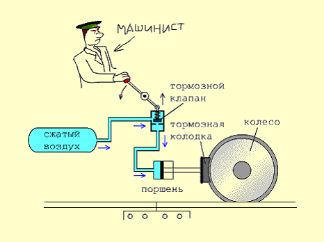
Now let's ask ourselves, would the driver be able to stop the train if the brake lever was directly connected to the brake pads? Probably, not. No matter how strong he is, a person cannot stop a train. And compressed air does this easily, you just need to open the valve.
Let's see what happened: the driver spends little energy pressing the brake lever. The valve opens and a powerful flow compressed air, with much more energy, presses the brake pads. That is, the valve can be called a reinforcing element that enhances the weak energy expended by a person due to the strong energy of compressed air.
I dare to assure you that everything is absolutely the same in a transistor. Only it is not compressed air that passes through it, but electricity. The transistor has three terminals: collector, emitter and base.

A strong current flows between the collector and the emitter, it is called the collector current (Ik), between the base and the emitter there is a weak control current of the base (Ib). The magnitude of the collector current depends on the magnitude of the base current, just as the pressure of compressed air depends on how open the valve is. Moreover, the collector current is always greater than the base current by a certain number of times. This value is called the current gain, denoted h21e. U various types For transistors, this value ranges from a few to hundreds of times.
So, the current gain is the ratio of the collector current to the base current:
h21e = Ik / Ib
In order to calculate the collector current, you need to multiply the base current by the gain:
Ik = Ib * h21e
Let's draw a diagram.

In this circuit, a transistor controls the brightness of the light bulb. In other words, it regulates the current flowing through the light bulb. Since the light bulb is connected to the collector of the transistor, the current flowing through it is the collector current.
The base control current is limited by resistor R1. Knowing this current and the gain of the transistor (h21e), you can easily find out the collector current. On the other hand, knowing what collector current we need, we can always calculate the base current and select the appropriate resistor.
Let's do some math :)
.Let our light bulb consume a current of 0.33 A,
and the transistor has h21e = 100.
What base current is needed for the light bulb to burn at full intensity?
And what will be the resistance R1?
Full heat is when the current consumption is equal to the rated current.
Nominal - 0.33 A. Thus, the required collector current is 0.33 A.
The base current should be less than the collector current by a factor of h21e. That is, 100 times. That is, it should be equal to 0.33/100 = 0.0033A = 3.3 mA.
Hurray, we decided!!!