SMD ( S urface M mounted D evice), which translated from English means “surface-mounted device.” In our case, the surface is a printed circuit board.
These are the type of printed circuit boards where SMD components are installed. SMD components are not inserted into the holes of the boards, they are soldered onto contact tracks (I call them patches), which are located directly on the surface printed circuit board. The photo below shows the tin colored pads on a mobile phone circuit board after all the SMD components have been removed.
In our turbulent age of electronics, the main advantages of an electronic product are small size, reliability, ease of installation and dismantling (disassembling equipment), low energy consumption and convenient usability ( from English- Ease of use). All these advantages are by no means possible without surface mount technology - SMT technology ( S urface M ount T echnology), and of course without SMD components. But why? Let's take a closer look at this issue.
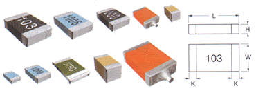
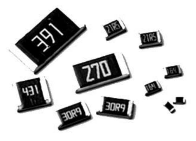
The most important advantages of SMD components are, of course, their small dimensions. The photo below shows simple resistors and SMD resistors.
![]()
Due to its small dimensions, it is possible to place more SMD components per unit area than simple ones. Consequently, the installation density increases and, as a result, the dimensions decrease electronic device. And since the weight of an SMD component is many times lighter than the weight of the same simple component, the weight of the radio equipment will also be many times lighter.
SMD components are much easier to desolder; for this we need a soldering station with a hair dryer. You can read how to desolder and solder SMD components in the article How to solder SMDs correctly. It is much more difficult to solder them; in production they are placed on a printed circuit board by special robots. No one solders them manually in production, except for radio amateurs and radio equipment repairmen.
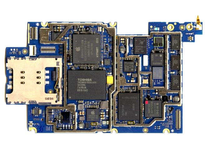
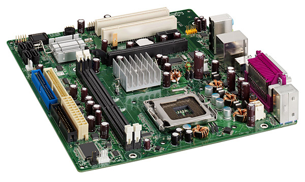
Since equipment with SMD components has a very dense installation, there should be more tracks on the board. But the tracks do not fit on one surface, so printed circuit boards are made multilayer. If the equipment is complex and the density of components is very high, then the board will therefore have more layers. It's like a multi-layer cake made from short layers. This means that the printed traces connecting the SMD components are located directly inside the board and cannot be seen in any way. Example of multilayer boards - boards mobile phones and computer or laptop boards (motherboard, video card, RAM). In the photo below the blue board is the Iphone 3g, the green board is the computer's motherboard.
All radio equipment repairers know that if a circuit board overheats, it will swell with a bubble. In this case, the interlayer connections break and the board becomes a complete mess without any restoration. Therefore, the main trump card when replacing SMD components is the correct temperature.
Some boards use both sides of the printed circuit board, and the mounting density, as you understand, doubles. This is another advantage of SMT technology. Oh yes, it’s also worth taking into account the fact that the material required for the production of SMD components is much less, and their cost during mass production of millions of pieces literally costs pennies. In short, only advantages :-). But, since there are advantages, there must also be disadvantages... But they are very insignificant, and actually do not concern us. This is expensive equipment and technology in the production and development of SMD components, as well as the accuracy of soldering temperature.
What should you use in your designs? If your hands don’t shake and you want to make, say, a small radio bug, then the choice is obvious. But still, in amateur radio designs, dimensions do not play a big role, and soldering massive radio elements is easier and more convenient. Some radio amateurs use both mixed in ;-).
Let's look at the main SMD elements used in our modern technologies. Resistors, capacitors, low-value inductors, fuses, diodes and other components look like ordinary rectangles.
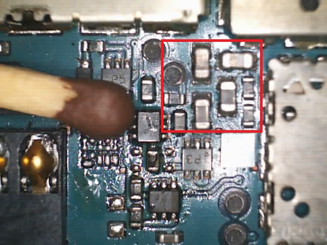
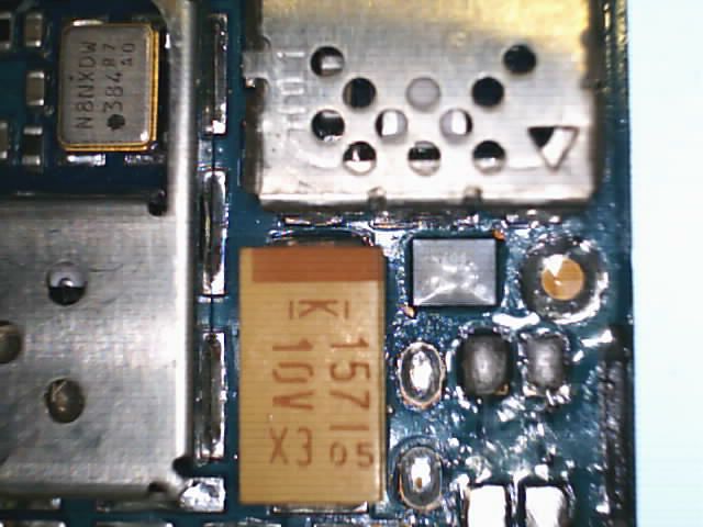
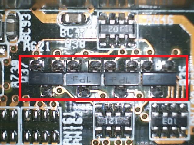
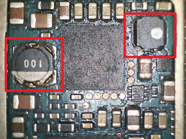
On boards without a diagram it is impossible to guess whether it is a resistor, or a condenser, or who knows what. On large SMD elements they still put a code or numbers to determine their characteristics and parameters. In the photo below these elements are marked in a red rectangle. Without a diagram for the device, it is impossible to say what elements these are.
The standard sizes of SMD components may be different. This depends on the technical characteristics of these components. Basically, the higher the component's value, the larger it is in size. Here is a description of the standard sizes for resistors and capacitors. Here, for example, is a rectangular SMD capacitor yellow color. They are also called tantalum or simply tantalum:
And this is what SMD transistors look like:
There are also these types of SMD transistors:
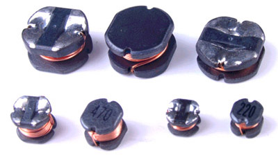
Inductors, which have a high rating, in SMD version look like this:
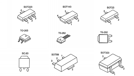
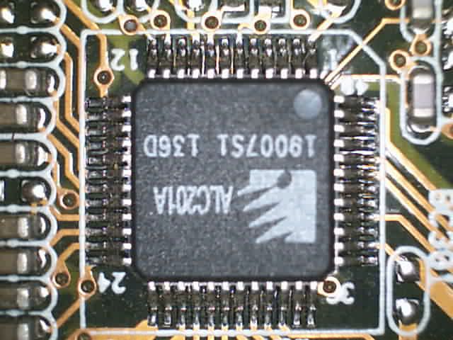
And, of course, how could we live without microcircuits in our age of microelectronics! There are many SMD types of chip packages, but I divide them mainly into two groups:
1) Microphones in which the leads are parallel to the printed circuit board and are located on both sides or along the perimeter.
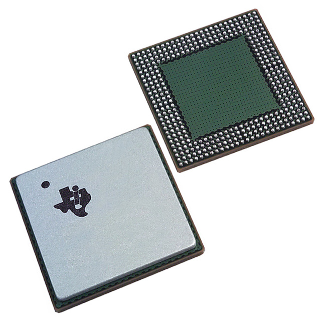
2) Microphones whose conclusions are located under the microcircuit itself. This is a special class of microcircuits called BGA (from English Ball grid array- an array of balls). The terminals of such microcircuits are simple solder balls of the same size. In the photo below is the micra itself, and its reverse side, consisting of ball leads. BGA chips are convenient for manufacturers because they save a lot of space on the printed circuit board, because there can be thousands of such balls under some BGA microchip, which makes life much easier for manufacturers, but does not make life any easier for repairmen :-).
We can talk a lot more about SMD technology and components. In this article I outlined mainly superficial review world of SMD components. Every day new gadgets and components are being developed. Smaller, thinner, more reliable. Some novice electronics engineers are indignant, saying: “Why the hell do they tell us at school, at the university or somewhere else about some kind of Soviet transistors or old Soviet diodes, why do we need this, after all, this is the age of microelectronics?” This is where they are mistaken... A diode, it is a diode in Africa, be it SMD or Soviet, the difference is in the dimensions. But it will work exactly the same as the Soviet one. Just know that microelectronics comes from the word “micros”, which means “small” in Latin, but the laws of electronics are the same everywhere, whether in a large radio element or in a tiny SMD.
We have already become acquainted with the main radio components: resistors, capacitors, diodes, transistors, microcircuits, etc., and also studied how they are mounted on a printed circuit board. Let us once again recall the main stages of this process: the leads of all components are passed into the holes in the printed circuit board. After which the leads are cut off, and then with reverse side The boards are soldered (see Fig. 1).
This process, already known to us, is called DIP editing. This installation is very convenient for beginner radio amateurs: the components are large, they can be soldered even with a large “Soviet” soldering iron without the help of a magnifying glass or microscope. That is why all Master Kit kits for do-it-yourself soldering involve DIP mounting.
Rice. 1. DIP installation
But DIP installation has very significant disadvantages:
Large radio components are not suitable for creating modern miniature electronic devices;
- output radio components are more expensive to manufacture;
- a printed circuit board for DIP mounting is also more expensive due to the need to drill many holes;
- DIP installation is difficult to automate: in most cases, even large factories In electronics production, installation and soldering of DIP parts must be done manually. It is very expensive and time consuming.
Therefore, DIP mounting is practically not used in the production of modern electronics, and it has been replaced by the so-called SMD process, which is a standard today. Therefore, any radio amateur should have at least a general idea about it.
SMD mounting
SMD (Surface Mounted Device) is translated from English as “surface mounted component”. SMD components are also sometimes called CHIP components.
The process of mounting and soldering chip components is correctly called the SMT process (from the English “surface mount technology”). Saying “SMD installation” is not entirely correct, but in Russia this version of the name of the technical process has taken root, so we will say the same.
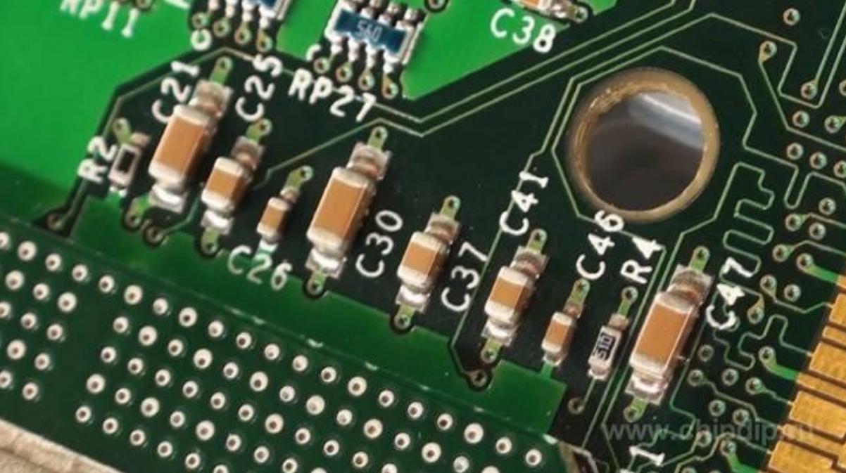
In Fig. 2. shows a section of the SMD mounting board. The same board, made on DIP elements, will have several times larger dimensions.
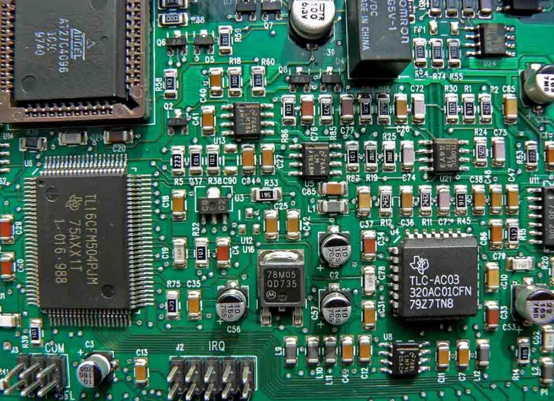
Fig.2. SMD mounting
SMD installation has undeniable advantages:
Radio components are cheap to produce and can be as miniature as desired;
- printed circuit boards are also cheaper due to the absence of multiple drilling;
- installation is easy to automate: installation and soldering of components is carried out by special robots. There is also no such technological operation, like cutting leads.
SMD resistors
It is most logical to start getting acquainted with chip components with resistors, as the simplest and most widespread radio components.
SMD resistor in its own way physical properties is similar to the “usual” inferential version we have already studied. All its physical parameters (resistance, accuracy, power) are exactly the same, only the body is different. The same rule applies to all other SMD components.
Rice. 3. CHIP resistors
Standard sizes of SMD resistors
We already know that output resistors have a certain grid of standard sizes, depending on their power: 0.125W, 0.25W, 0.5W, 1W, etc.
A standard grid of standard sizes is also available for chip resistors, only in this case the standard size is indicated by a four-digit code: 0402, 0603, 0805, 1206, etc.
Basic sizes of resistors and their specifications are shown in Fig. 4.

Rice. 4 Basic sizes and parameters of chip resistors
Marking of SMD resistors
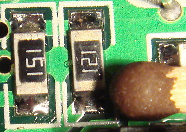
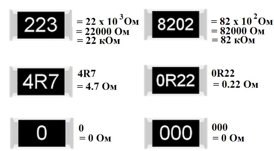
Resistors are marked with a code on the case.
If the code has three or four digits, then the last digit means the number of zeros. In Fig. 5. resistor with code “223” has the following resistance: 22 (and three zeros to the right) Ohm = 22000 Ohm = 22 kOhm. Resistor code "8202" has a resistance of: 820 (and two zeros on the right) Ohm = 82000 Ohm = 82 kOhm.
In some cases, the marking is alphanumeric. For example, a resistor with code 4R7 has a resistance of 4.7 Ohms, and a resistor with code 0R22 has a resistance of 0.22 Ohms (here the letter R is the separator character).
There are also zero resistance resistors, or jumper resistors. They are often used as fuses.
Of course, you don’t have to remember the code system, but simply measure the resistance of the resistor with a multimeter.
Rice. 5 Marking of chip resistors
Ceramic SMD capacitors
Externally, SMD capacitors are very similar to resistors (see Fig. 6.). There is only one problem: the capacitance code is not marked on them, so the only way to determine it is to measure it with a multimeter that has a capacitance measurement mode.
SMD capacitors are also available in standard sizes, usually similar to resistor sizes (see above).
Rice. 6. Ceramic SMD capacitors
Electrolytic SMS capacitors
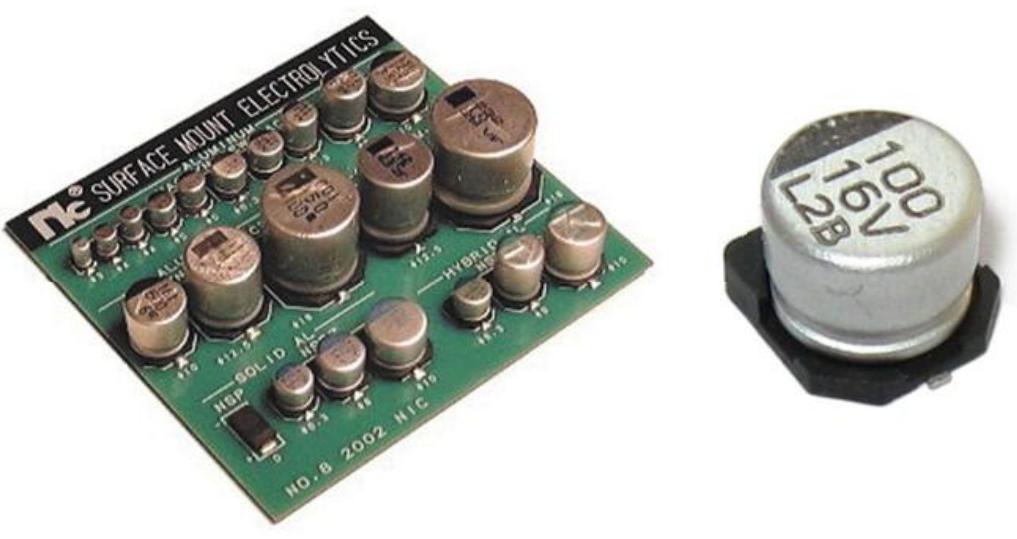
Fig.7. Electrolytic SMS capacitors
These capacitors are similar to their lead counterparts, and the markings on them are usually clear: capacitance and operating voltage. A stripe on the cap of the capacitor marks its negative terminal.
SMD transistors
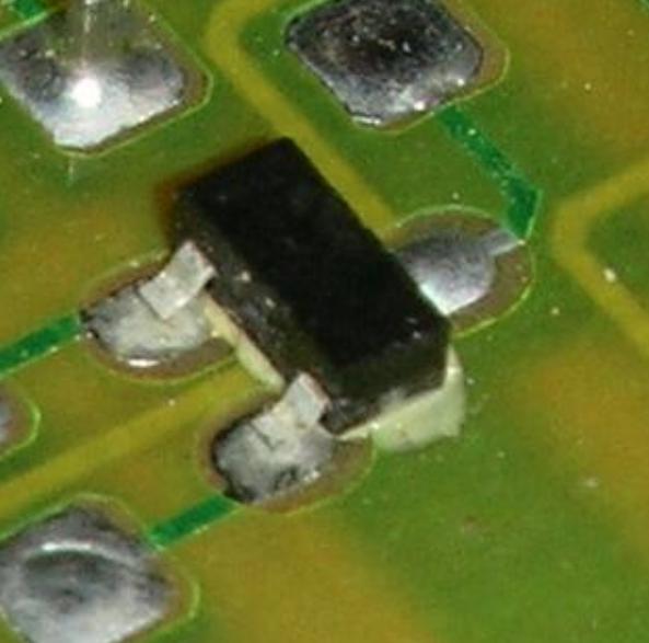
Fig.8. SMD transistor
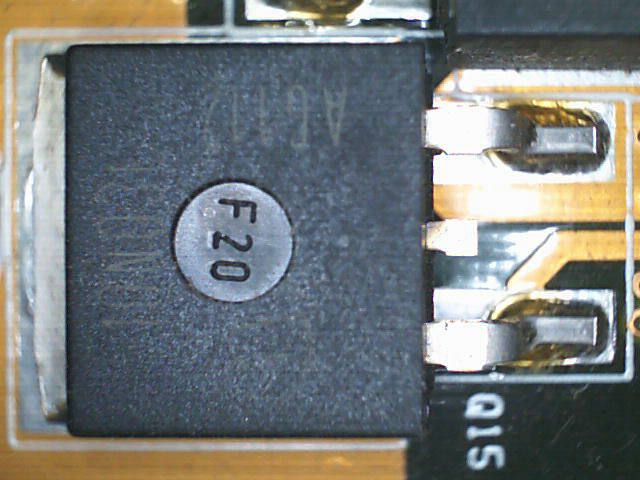
Transistors are small, so it is impossible to write their full name on them. Are limited to code marking, and some international standard no markings. For example, code 1E may indicate the type of transistor BC847A, or maybe some other one. But this circumstance does not bother either manufacturers or ordinary consumers of electronics at all. Difficulties can only arise during repairs. Determining the type of transistor installed on a printed circuit board without the manufacturer's documentation for this board can sometimes be very difficult.
SMD diodes and SMD LEDs
Photos of some diodes are shown in the figure below:
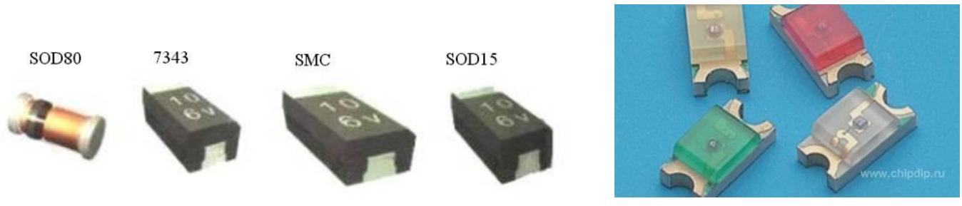
Fig.9. SMD diodes and SMD LEDs
The polarity must be indicated on the diode body in the form of a stripe closer to one of the edges. Usually the cathode terminal is marked with a stripe.
An SMD LED also has a polarity, which is indicated either by a dot near one of the pins, or in some other way (you can find out more about this in the documentation of the component manufacturer).
Determining the type of SMD diode or LED, as in the case of a transistor, is difficult: an uninformative code is stamped on the diode body, and most often there are no marks at all on the LED body, except for the polarity mark. Developers and manufacturers of modern electronics care little about their maintainability. It is assumed that the printed circuit board will be repaired by a service engineer who has complete documentation for a specific product. Such documentation clearly describes where on the printed circuit board a particular component is installed.
Installation and soldering of SMD components
SMD assembly is optimized primarily for automatic assembly by special industrial robots. But amateur radio designs can also be made using chip components: with sufficient care and attention, you can solder parts the size of a grain of rice with the most ordinary soldering iron, you only need to know a few subtleties.
But this is a topic for a separate large lesson, so more details about automatic and manual SMD installation will be discussed separately.
SMD reference books
SMD - Abbreviation of in English, from Surface Mounted Device - A device mounted on a surface, that is, on a printed circuit board, namely on special contact pads located on its surface. The use of SMD components can significantly reduce the size and weight of any amateur radio design.
The reference book contains information on deciphering the codes of more than 34 thousand microcircuits, diodes and transistors, switching circuits are given and implemented convenient system information search
An extremely useful reference book in the amateur radio library, with a very clear search, contains information on almost all active radio components, microcircuits, transistors, diodes and others, including SMD.
Due to its very small dimensions, many novice radio amateurs have the question “How to solder SMD?”. In this short article we tried to answer this question using a practical example.
About SMDBut there are also disadvantages, firstly, soldering SMD components, the process is interesting and requires basic skills and experience. Secondly, if the SMD used in multilayer printed circuit boards, and located inside the latter, fails, it is simply not possible to replace it. And when dismantling and replacing surface radio components, it is necessary to strictly observe temperature regime, otherwise damage to the internal structure cannot be avoided.
Externally, SMD radioelements look like small rectangles with a code or digital designation. And only from them can one understand what it is: a resistor, capacitor, transistor or microcircuit. An SMD component in modern electronics can be any radio element. On very small SMDs, the code designation may be completely absent; in this case, only a diagram or service manual will help identify the element. The appearance of a printed circuit board with various SMD radio components is shown in the figure below: