Key element any product is its power supply, in this article we will look at PWM controllers that you can use in your designs to optimize power supply.
The basic circuit by which many low- and medium-power switching power supplies are made is a flyback converter. The main advantage of the flyback topology is its low cost and small number of components. Therefore, almost all network power supplies with a power of up to 30-50 W are built according to this topology. This circuit converts one DC voltage to another by adjusting the output voltage by pulse width modulation(PWM) or pulse frequency modulation (PFM). Pulse width modulation is a control method based on changing the ratio of the duration of the switch on to the off state at a constant frequency. In a flyback converter, the duration of the switch's on state is longer than the duration of the off state: in this case, a larger amount of energy is stored in the transformer and transferred to the load.
The ON Semi range currently includes over 40 types of Flyback PWM controllers. In fact, all chips are built on the basic architecture that was first used in the UC384x integrated PWM controller chip, developed more than 15 years ago. The chip is very popular among power supply developers and is still produced by many manufacturers, including ON Semi.
The main function of a PWM controller is to control the power transistor(s) located in the primary circuit of the pulse transformer and maintain the output voltage at a given level using a signal feedback.
The structure of modern PWM controllers provides and additional functions, increasing the efficiency and reliability of the power supply:
Limiting the current and duty cycle of pulses in the control circuit of power transistors;
Smooth start of the converter after power supply;
Built-in dynamic power supply from high voltage input voltage;
Control of the input voltage level with the elimination of “dips” and “overshoots”;
Short circuit protection in the power transformer circuit and output rectifier circuits;
Temperature protection of the controller, as well as the key element;
Blocking the operation of the converter at low and high input voltage;
Optimization of control for standby mode and mode with reduced current in the load (skipping cycles or switching to a lower conversion frequency);
Optimization of EMR level.
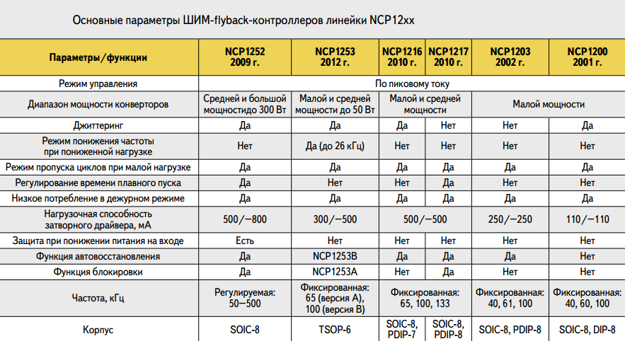
The PWM controllers we are interested in do not have a built-in power transistor that controls the current in the primary circuit of the power transformer. Let's look at the structure and parameters of PWM controllers of the Flyback topology, which are represented by the NCP12xx line and developed by ON Semi for Lately: these include NCP1216/17 and NCP1252/53 microcircuits. The structure of these controllers is further development architecture of the NCP1200/1203 line, developed in the early 2000s
It should be noted that the structure of the latest Flyback PWM controller microcircuits uses almost the same basic set of standard functional modules. The main differences are determined by the current load capacity of the output stage (from 110 to 800 mA), the frequency control mode (constant or variable frequency), as well as the operating logic when critical situations are detected. The structure of the PWM controller contains logic that defines the state machine. The transition machine circuit is implemented using comparators, flip-flops, timers and logic elements.
Basic controller states: initial start frequency generator, entering the operating mode, adaptive monitoring of the load current and selection of the optimal mode, detection of critical situations, transition to emergency mode, auto-recovery after failures. Most of the Flyback controller chips are made in compact 8-pin packages (SOIC-8, PDIP-8). Despite the similarity in structure, the purpose and location of the controller microcircuit pins for various types differ considerably. Before evaluating and comparing the parameters of new controllers, let's consider the main functions basic modules controller.
Protection and work safety
Network converters must provide a sufficient level of safety during operation without degradation of the characteristics of power elements in the event of current overloads, primarily due to short circuits in the transformer windings or in the load. A short circuit is detected by the sudden disappearance of the feedback signal through the optocoupler. The output transistor driver must be disabled to prevent the transistor from overheating and saturating the transformer. However, during the startup process, the feedback signal is also absent for some time. We need to identify these two situations.
Some inexpensive controllers do not provide output short circuit protection. In such cases, the occurrence of a current overload will lead to uncontrollable consequences and can lead to the destruction of the power elements of the converter in a matter of seconds. A short circuit can be of several types - in the load itself, the windings, the electrolytic capacitor of the output rectifier, rectifier diodes. The introduction of deterministic states increases the complexity of the machine, but increases the reliability of the converter.
Locking and auto-recovery function in emergency situations
Currently, several variants of scenarios for handling emergency situations that arise in power supplies based on Flyback PWM controllers are used. The transition to emergency mode when critical situations are detected can involve both forced current limitation and complete blocking of the converter operation. When blocked, the master PWM generator stops and the supply of an active signal to the power transistor is prohibited.
Depending on the type or modifications of the microcircuits, two blocking scenarios are possible. In the first case, after the lock is triggered, the converter “latches” in this state and does not change it, even if the condition that caused this state has already disappeared. Restoring the converter's operation is possible only after turning off the mains voltage and turning the power back on.
In the second case, attempts are made to automatically restore normal operation of the converter. To do this, a timer is started in the controller structure for a time of about 1.5 s. After this time has expired, the controller again checks for critical situations, and if they persist, the blocking remains. In this case led indicator network source will blink with a period of 1.5 s.
Input undervoltage protection
Reducing the voltage at the power input of the controller microcircuit below the threshold can primarily lead to incorrect operation of the driver that controls the power transistor. And this will lead to non-optimal and inconsistent operation of the power stage, overheating field effect transistor, transformer saturation and emergency current increase. The protection automatically blocks the operation of the generator and gate driver, thereby preventing an emergency. The protection module consists of a threshold comparator and a logic circuit that determines the operating algorithm of the protective module. For of this type protection can be used in latch or auto-recovery modes after termination emergency situation.
Low consumption in standby mode
In standby mode, there is practically no current in the load and the main consumption from the network will be through the power supply circuit of the controller logic. The controller microcircuits are powered through a resistor connected to the rectified mains voltage bus. The consumption of the entire power supply in standby mode will be determined by the amount of current flowing in this circuit. However, it cannot be made negligibly small, since it is necessary to ensure the operation of the logic during the initial startup of the converter during the transition from standby to operating mode. Modern controllers have ultra-low current consumption in standby mode - 100 µA or less.
Low Frequency Mode
The latest controllers use a Frequency foldback mode. This transition occurs when the feedback signal decreases below a threshold value. Lowering the conversion frequency allows you to reduce consumption in standby mode.
Skip cycle mode
The mode of skipping frequency cycles allows you to reduce consumption in standby mode. The mode is activated when the amplitude level of the feedback signal decreases below the set threshold. Skip-Cycle and Frequency foldback are implemented in one controller block module.
Reducing EMI due to jitter internal generator
For controllers operating at a fixed frequency, the technique of introducing small frequency modulation ±5% around the center frequency (jitter) can be used. The presence of jitter does not affect the operation of the converter, but it allows you to “blur” the EMI spectrum and thus reduce the amplitude of interference.
Feedback signal ramp compensation
NCP1216 - controller for network power adapters
The NCP1216 chip is available in SOIC-8 and PDIP-7 packages. It is an expanded version of the previously developed NCP1200 controller and is fully pinout compatible with it. Unlike the previous model, the NCP1216 microcircuit has an increased load capacity through the gate control channel of the power field switch. In addition, a function has been added to compensate for the decline in the current characteristic and a jittering function has been introduced (forced swing of the fundamental frequency of the built-in clock generator). This function ensures a reduction in EMI levels while maintaining high conversion efficiency. These innovations make it easier to design today's network power adapters.
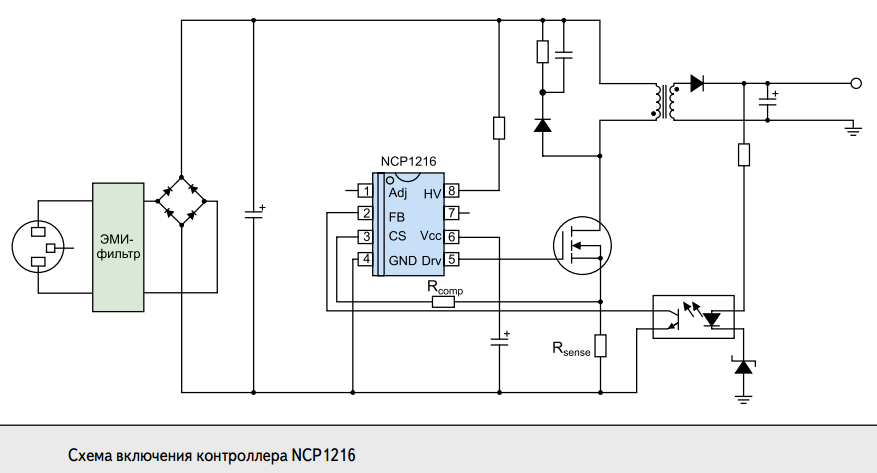
There are options for microcircuits with different fixed frequency values of the built-in oscillator, which provides a certain freedom of choice for the developer. The microcircuit is powered from rectified mains voltage and does not require additional windings of a pulse transformer to organize this power.
The NCP1216 controller has effective built-in protection modules that provide output shutdown in the event of abnormal output current values. In this case, the microcircuit goes into protected mode with cyclic restart attempts to resume normal mode after the current overload stops. There are different versions of microcircuits that differ in the algorithm of behavior when a current overload occurs: with automatic restoration of the operating state and restoration by turning off and turning on the power again. The developer, depending on the operating conditions of the power source, can select the desired version of the controller chip.
Main parameters of NCP1216:
No additional winding of a pulse transformer is required for power supply.
Current control mode with cycle skip adjustment at low load.
Internal droop compensation.
Limited duty cycle to 50% (NCP1216A version only).
Internal soft start delay of 1 ms (NCP1216A only).
Swinging the frequency of the master oscillator to reduce the EMI level.
Auto-recovery mode after current overload at the output.
Output short circuit protection.
Low consumption of internal logic in standby mode.
Output load current capacity: 500 mA.
Versions with fixed clock frequencies: 65/100/133 kHz.
Internal overheat protection.
Direct connection to optocoupler.
A SPICE model is available for simulation.
Pin-to-pin compatible with NCP1200 series controller.
Typical Applications:
High power network adapters for LCD TVs, satellite receivers and other home audio/video equipment.
Network adapters for laptops (with standby mode).
DC/DC converters for telecommunications equipment.
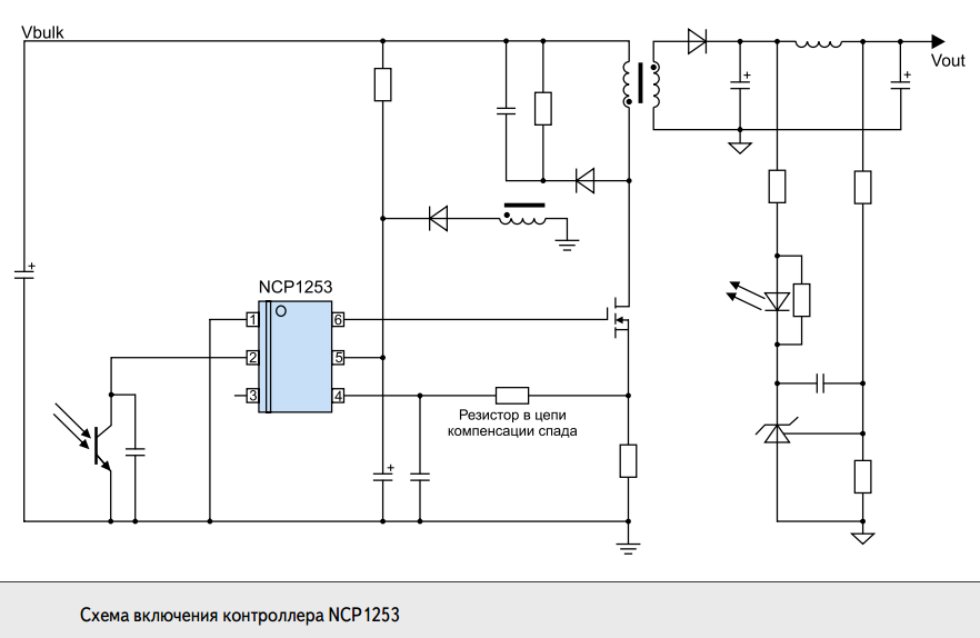
NCP1217 controller chip
The NCP1217 chip in a custom package (SOIC-7 or PDIP-7) represents the next generation of controllers that develop the NCP1203 architecture. The NCP1217 design uses an external field switch gate driver with increased current carrying capacity. In addition, a droop compensation circuit has been introduced, and an output overvoltage protection circuit has been added, which generally increases the reliability of the chip and the entire power supply and facilitates the development of the power supply. The NCP1217 controller can be used as an alternative to the well known and widely used UC384X series controller.
The internal clock generator can operate at one of three fixed frequencies (65, 100, 133 kHz) for different versions microcircuits. An internal droop compensation circuit prevents the occurrence of subharmonic oscillations that are very common in continuous conduction mode. The microcircuit also implements a transition to a mode with skipping cycles with a significant decrease in the current in the load.
The NCP1217 controller implements two effective protection modules:
Protection when short circuit and current overload at the output, in which the supply of control pulses to the power switch is blocked, the controller goes into safe mode with periodic restart attempts. By default, auto-recovery of normal mode after an emergency is used.
Input of operation blocking signal from an external source. The presence of this input allows, for example, to control the temperature of external power circuits, in particular, in the load itself, and in an emergency, directly block the converter without waiting for its own protection to operate.
SHIM-controller NCP1252
The NCP1252 controller is mainly aimed at using computer network power supplies in ATX. There is an input undervoltage protection function, which ensures safe work in various modes. The microcircuit is not compatible in terms of pins and connection circuit with versions of NCP1216/NCP1217 controllers.
Main parameters:
Peak current regulation mode.
Adjustable frequency of the converter: up to 500 kHz.
Frequency sweep range (for jitter): ±5% of the fundamental frequency.
Inrush current protection when turned on (fixed turn-on delay of 10 ms).
The switch-on delay is carried out through an internal timer and does not require external timing elements.
Adjustable soft start timer.
Auto-recovery mode when detecting a voltage drop at the output below the permissible value.
The UVLO protection threshold is set as for the UC384X series microcircuits.
Supply voltage range of the microcircuit: from 9 to 28 V (there is an auto-recovery function when the input power decreases).
Internal adjustable droop compensation.
Gate driver load capacity: +500/–800 mA.
Limiting the duty cycle of the output gate control pulses:
* maximum 50% (version A);
*maximum 80% (version B).
SOIC-8 package.
Typical applications are power supplies for personal computers.
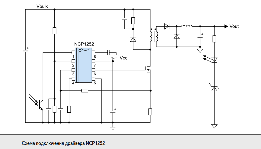
Choice of frequency, as well as the ability to work on high frequencies(up to 500 kHz) allow you to optimize various parameters network converter, depending on the requirements for both electrical parameters(efficiency, output power, maximum current, input voltage range), and to the dimensions of the transformer and the space occupied on printed circuit board. The high load capacity of the gate driver (up to 800 mA) with high efficiency (operation at 500 kHz) allows the Flyback topology to be used for designing economical network sources of medium and high power, primarily power supplies for computers.
6-pin PWM controller NCP1253
The NCP1253 is a fixed-frequency PWM controller designed for low-power AC adapters under 50 W. A special feature of the controller is the ultra-compact TSOP-6 housing with a minimum number of pins. In reality, out of the six pins of the TSOP-6 package, only five are used:
1-Power supply for the microcircuit.
3-Feedback signal.
4-Output power switch control signal.
5-Current sensor/connection of the droop compensation circuit.
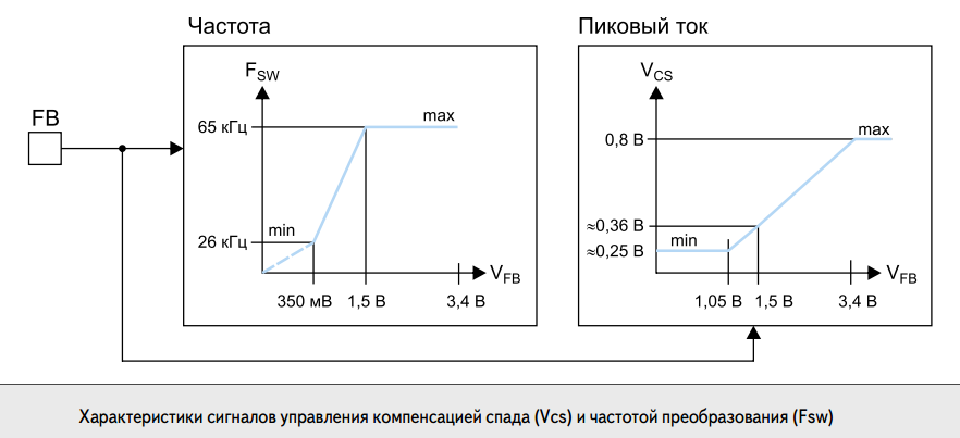
The chip can be used in compact and low-cost network power supplies of low and medium power. Accordingly, it has an optimized set of functional modules. There is no input voltage monitoring function to implement undervoltage protection. The frequency is not adjustable: two fixed values are set (65 and 100 kHz) for two versions of the microcircuit A and B. The soft start period is fixed and not adjustable, as in NCP1252. The current of the output gate driver of the power transistor is significantly less. Operation in standby mode and in a wide range of load changes is allowed. The microcircuit implements the function of reducing frequency and skipping cycles with a significant reduction in the current in the load, while maintaining high conversion efficiency for the entire range of load changes.
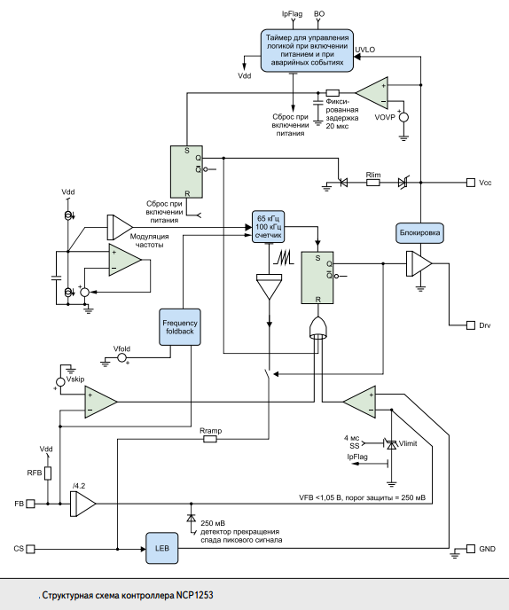
Main parameters:
Fixed internal oscillator frequencies: 65/100 kHz.
Control mode - current.
Downshift mode up to 26 kHz and skip cycle mode for light loads.
Adjustable droop compensation.
Gate driver load capacity: +300/–500 mA.
Soft start: 4 ms.
Auto-recovery mode (with timer) or latching in case of short circuit at the output.
Frequency swing of the master oscillator, as well as the transition mode to low frequency with a sharp decrease in load current.
Input overvoltage protection.
Supply voltage: up to 28 V
Ultra-low consumption of internal logic in standby mode.
Typical Application:
Network adapters for LCD TVs, satellite TV receivers, printers.
External network adapter for laptops and netbooks.
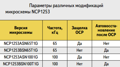
The NCP1253 chip uses a standard current-controlled architecture, where the phases of the power switch states are determined by the value of the peak current threshold. The NCP1200 series architecture continues to evolve, and the NCP1253 controller contains all the components needed to implement a modern and reliable power supply, including supply overvoltage protection, as well as an adjustable droop compensation signal. The microcircuit has a very low current consumption in standby mode - only 15 μA. There are four different versions, which differ in the frequency of operation of the internal generator, as well as in the scenarios of operation of the protection during current overload.
The modern power supply market offers the developer wide choose various products electronics, each of which is, to one degree or another, ready to solve the problems assigned to engineers. This article aims to review and help you choose optimal solutions from the proposals of the most famous players in the switching power supply market.
Introduction
Previously, power systems in functional diagram At the design stage, attention was often paid only to the final stage; many experts underestimated their ability to improve the product as a whole. Recently, trends in the development of the electronics industry have brought to the forefront for developers such tasks as reducing energy consumption, weight and size characteristics, development time and final cost products. Such requirements have changed the once secondary attitude towards the power supply units of the device, because in many respects the ability of the final product to be competitive and withstand stringent market requirements depends on them.
Today, the leading position in this area is traditionally occupied by Power Integration. The products of this company are well known, the application technology has been proven many times, which is the factor that tips the scales in its favor.
As competing products, consider the power supply offering from Fairchild Semiconductor. This company has long established itself in the field of power electronics, offering inexpensive, high-quality and multifunctional solutions. As a rule, the products of this manufacturer are focused on areas that require a high degree of reliability and performance.
Power supplies
Virtually all products in the electronics industry require power. DC from battery or power source. In addition, most devices have increased requirements for its quality. The voltage must be regulated and protected from ripples that occur. There are three types of power converters:
- DC\DC converter;
- AC\DC power supply;
- DC\AC inverter.
An ideal source should generate the required voltage values, despite changes in ambient temperature, load or input voltage. Moreover, it must be 100% effective. In Fig. 1 you can see the shortcomings of the real power supply.
Rice. 1. Real power supply
Today there are linear and. Pulse conversion is interesting because high efficiency and power density. The table compares some of the main features of linear and switching power supplies. Voltage and current stability is usually better with linear power supplies, sometimes by an order of magnitude, but switching power supplies often use linear output stabilizers that improve the output voltage parameters.
Table. Comparison of switching and linear power supplies
Finally, switching power supplies have more wide range input voltages. The input voltage range of linear power supplies usually does not exceed 10% of the rated value, which has a direct impact on efficiency. For pulsed sources, the effect of changing the input voltage on the efficiency is very small or absent altogether, and a wide operating range of input voltages makes it possible to work with large changes in the mains voltage (up to 40%). The most frequently used (due to its advantages) is the scheme flyback converter(Fig. 2). Many microcircuits for controlling these converters have been developed. There are both microassemblies that use an external power transistor, and those that include power element into its composition, which reduces its dimensions.
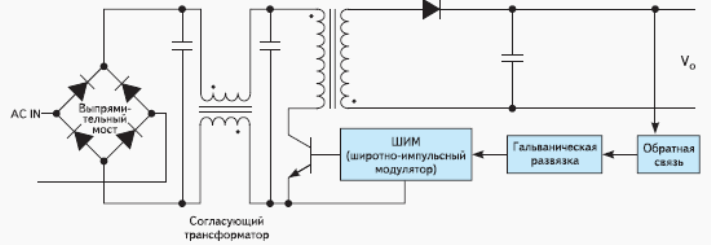
Rice. 2. Diagram of a flyback converter with a matching transformer and galvanic isolation
In the recent past, the implementation of pulse width modulation and performance monitoring was carried out using discrete elements. The emergence of integrated circuits that take on these functions has greatly simplified the development process and reduced costs several times. dimensions power supplies (Fig. 3). Leaders in the production of power supply control integrated circuits are Power Integrations and Fairchild Semiconductor.
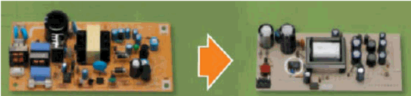
Rice. 3. Evolution of power supplies
Power Integrations Voltage Regulators
PNY* - Core Independent Peripheral in Microchip microcontrollers, also known as CIP - Core Independent Peripheral.
Microcontrollers in switching power supplies
Part 1
Looking ahead, I would like to note that the purpose of this article is not to discuss the advantages or disadvantages of control methods, nor to provide recommendations on the selection of optimal topologies for constructing Switching Power Supplies (SMPS) and the calculation of circuit elements - there are tons of specialized literature for this.
The purpose of the article is to show the fundamental possibility of implementing most SMPS topologies on the universal peripherals of Microchip microcontrollers, to demonstrate the advantages of microcontroller solutions in terms of flexibility and versatility relative to specialized “analog” PWM controllers and ASICs for SMPS.
Below we will consider solutions based on microcontrollers, but such solutions cannot be called “digital” sources, since the feedback loop is still closed through analog blocks and the parameters of the PWM signal are formed by the hardware feedback loop, and are not calculated by the processor core. For fully digital solutions, Microchip produces specialized 16-bit digital signal controllers (dsPIC33 GS-series families).
What is the SMPS made of?
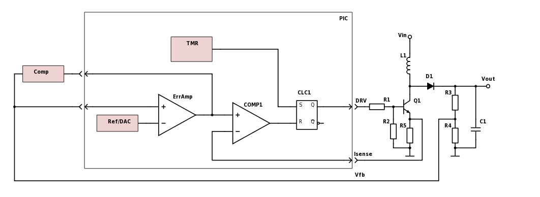
With my heart pulse source The power supply is provided by a PWM controller. Structural scheme One of the options for a specialized PWM controller is shown in Fig. 1.
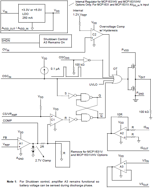
Fig.1. Structure of a specialized power converter driver chip.
The main element of the circuit is the SR flip-flop, which controls the output stage of the power switch.
The trigger is triggered by clock signals (input S, Set). The reset (input R, Reset) is controlled by the signals of the comparator C1, the reference signal for which is generated by the operational amplifier of the error signal A1. The trigger output controls the output switches, the control of which can be blocked by overvoltage signals (comparator C2), blanking, etc.
If it is necessary to control such or a similar circuit from the outside (changing and measuring parameters, soft start, etc.), you need to use external control solutions, for example a microcontroller or control logic.
In total, to build a controlled intelligent power supply, we need to have a PWM controller chip and a microcontroller, or we can combine it - using a microcontroller to make a PWM controller for an energy converter.
SMPS topologies
Topology is the connection of inductance, capacitor, switching circuit elements to ensure energy conversion, the ratio of input and output parameters.
| scheme | description |
|---|---|
 |
increasing |
 |
downward |
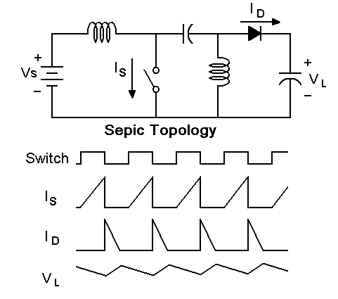 |
Sepic |
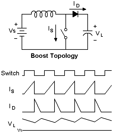
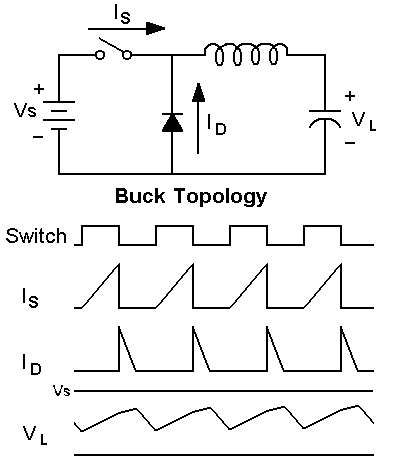
Rice. 2 Basic topologies of SMPS.
The principle of power switch control in the most commonly used SMPS topologies is generally the same (see Figure 2). The duty cycle of opening the power switch is adjusted, i.e. the relationship between the states “open” and “closed”. The duty cycle is controlled either depending on the output voltage (voltage-mode control) or depending on the current in the power inductance (current-mode control).
In each of the two modes, control can be hysteretic (Hysteretic Control) or proportional (Proportional Control). With hysteresis control, the duty cycle of the pulses is fixed, and the output voltage is adjusted by turning on or off the supply of control pulses of the power switch.
With proportional control, the duty cycle changes in proportion to the magnitude of the mismatch between the actual output voltage and the required one.
For common SMPS topologies, the industry produces specialized PWM controllers. But what to do if there is no ready-made PWM controller for the desired topology? In this case, a microcontroller with configurable peripherals can also come to the rescue.
Microcontrollers with PNY
Let's consider the composition of the peripherals of 8-bit Microchip microcontrollers intended for building energy converters.
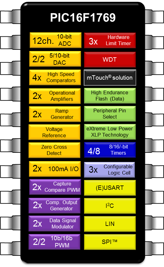
Rice. 3. Peripherals of PIC16F1769 series controllers
PIC16F176x series controllers (see Fig. 3) have a set of peripheral modules sufficient to implement multi-channel PWM switching power supply controllers:
- fast comparators;
- operational amplifiers;
- complementary signal generator (COG);
- programmable ramp generator (PRG);
- reference voltage source;
- zero crossing detector (ZCD);
- timers with reset and limit functions, PWM;
- signal modulator;
- Configurable Logic Cells (CLC);
- temperature sensor.
Peripheral modules can be connected within the microcontroller to perform specific functions. For example, Figure 4 illustrates the configuration of peripherals to perform the power converter function. Moreover, such configured relationships between peripheral modules do not require kernel intervention during device operation.
Rice. 4. Boost LED power converter with current stabilization and dimming.
Thus, on one chip/microcontroller we can implement the core of a switching power supply and control logic (program), thereby we are able to exclude a specialized power converter driver from the circuit.
Let's take a closer look at the various operating modes of PWM controllers and the possibility of implementing them on the periphery of Microchip microcontrollers.
Voltage Mode
In this mode, the duty cycle of the PWM signal controlling the power switches is determined directly by the output voltage.
With hysteresis control, if the output voltage is below normal, the source is “pumped”. If the output voltage is greater than the threshold, the comparator blocks control of the power switch, and the output discharge occurs storage capacity. In English-language literature, this mode is called “hiccup-mode” - “mode with hiccups.”
This mode is used relatively rarely, as it is accompanied by large ripples in the output voltage and requires a storage capacitor of relatively high capacity.
Figure 5 shows the operating principle of the voltage control mode with hysteresis control. Here and below, the output part of the source is not shown, since it is determined by the topology, output power, etc. To illustrate the principle of operation of a PWM controller, an example with the output part will sometimes be shown.
Rice. 5a. The first circuit is with a fixed output voltage, the second is with adjustable output voltage.
Rice. 5 B. Diagrams of PWM output and comparator output.
Rice. 6. An example of the output stage of a step-up switching power supply connected to a PWM controller (see Fig. 5).
Configurable logic cells (CLC) in Fig. 5 can be included as an AND element. To prevent high-frequency generation from the comparator, it is advisable to pass its output through another CLC - a D-trigger synchronized with a PWM signal. In this case, we get two “bonuses” - the absence of high-frequency generation and the unchanged duty cycle of the control PWM (see explanations in Fig. 7). For more information about configurable logic cells, see the article “Configurable logic cells in PIC microcontrollers”.
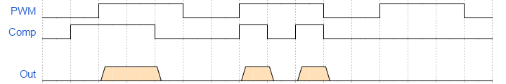
Fig.7.a. Shortening control PWM pulses, the possibility of high-frequency generation
Rice. 7.b. Signal synchronization prevents shortening of PWM pulses

Rice. 8. Signal synchronization to prevent PWM generation and shortening.
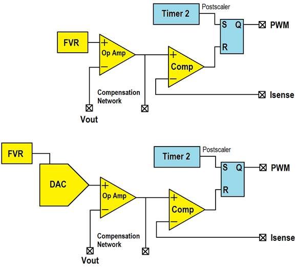
Voltage control with proportional control
In voltage control with proportional control, the output voltage mismatch must correct the duty cycle of the control pulses. The proportion between the mismatch value and the duty cycle correction value is provided by the error amplifier and the control loop filter. Voltage control with proportional control is used relatively rarely, since with this control method the inductance can go into saturation when the source is started and when the output is short-circuited, a second-order loop filter is required, and there is an influence of the input voltage on the gain of the error amplifier.
Voltage control with proportional control can be implemented on the built-in periphery of PIC controllers using a PWM modulator - you need a saw generator (Ramp generator) and a comparator (we have already considered the implementation of PWM modulators in). The reference PWM generated by the microcontroller serves to generate a sawtooth voltage and determines the frequency of control pulses, and the feedback voltage determines the duty cycle of control pulses.
To prevent saturation of the inductance when starting the source or during a short circuit at the output, it is necessary to limit the duty cycle of the control signal. To do this, the output signal of the comparator (CMP1_out) is fed to the CLC (AND element), and the reference PWM of saw formation is fed to the other input (PWM signal Fig. 10). The duration of the PWM pulse will serve as a duty cycle limiter for the DRV control signal (limit the signal from the comparator output).
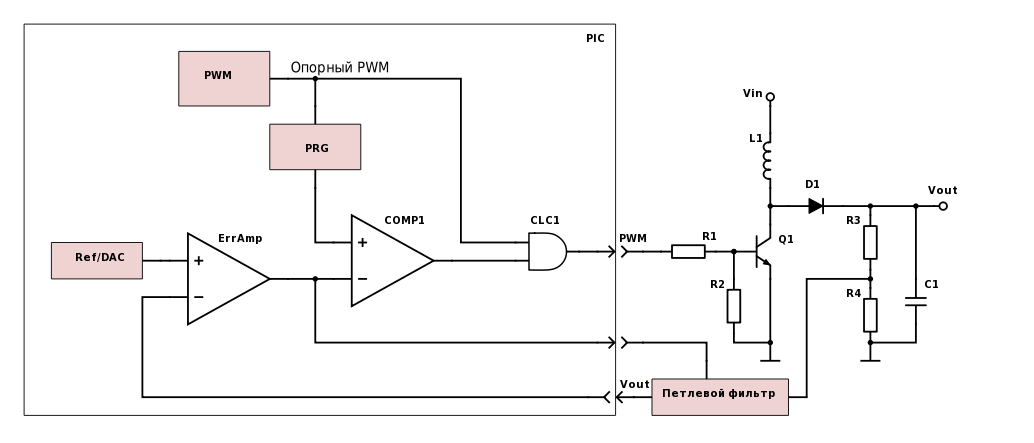
Fig.9 PWM SMPS controller in voltage control mode with proportional control.
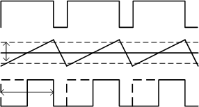
Fig. 10. Diagrams of operation of a PWM controller with voltage control
Current Control (Current Mode)
This method eliminates the disadvantage of voltage control mode. In this method, the Controller receives a second feedback loop. The internal fast circuit serves to control the power switch current (inductance) at each turn-on cycle. When a signal is given to open the power switch, the current through the inductance, and therefore through the power switch, begins to increase linearly. When the threshold is reached, the power switch opens, and the release of inductive energy through the diode begins. Based on time or upon detection of zero current in the inductance (in continuous current or critical conductivity mode, CCrM), the cycle is repeated.
Since the power switch opens when the peak current is reached, the stored energy in the inductance is ensured to remain constant regardless of the input voltage (a change in the input voltage affects the charging rate). The second control loop controls the output voltage.
Current control with hysteresis control: similar to the voltage control method - On/Off PWM control of the power switch is carried out depending on the output voltage.
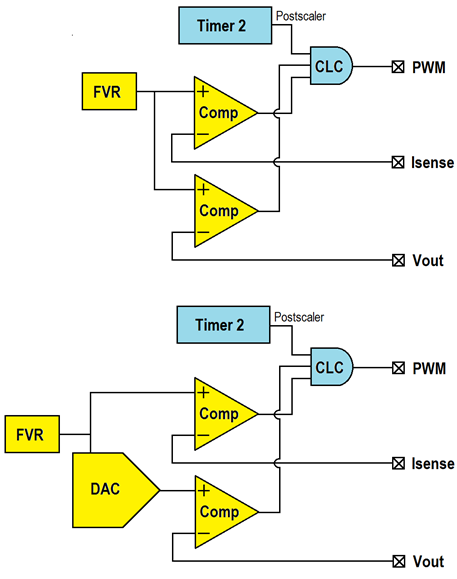
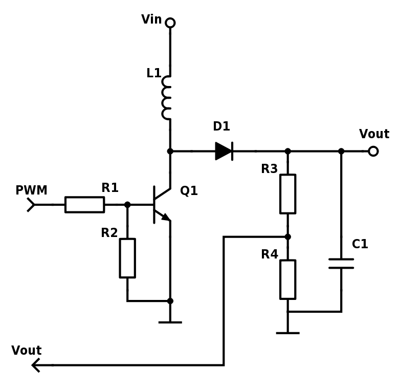
Fig. 11a. PWM controller with current control with hysteresis control. Isence – control of the Is current peak through inductance, Vout – checking the output voltage, blocking the control PWM if the output voltage is exceeded. Option with fixed output voltage and adjustable output voltage.
Rice. 11b. PWM controller and output topology option for boost converter with peak current control.
Current control with proportional control
With this control method, the variable duty cycle of the PWM depends on the output voltage and the active feedback filter.
Rice. 12. PWM controller with current control and proportional control. Fixed and adjustable output voltage options.
In this method, instability of the reverse loop is observed at a duty cycle above 50% (the appearance of generation at a frequency of ½ Fswx depends on the noise on Vin or Vout). This process has been well studied and the problem is solved by reducing the gain in the feedback loop, which can be achieved in two ways (Fig. 13):
- adding a sawtooth voltage to Isense;
- by subtracting the ramp voltage from the loop filter output.
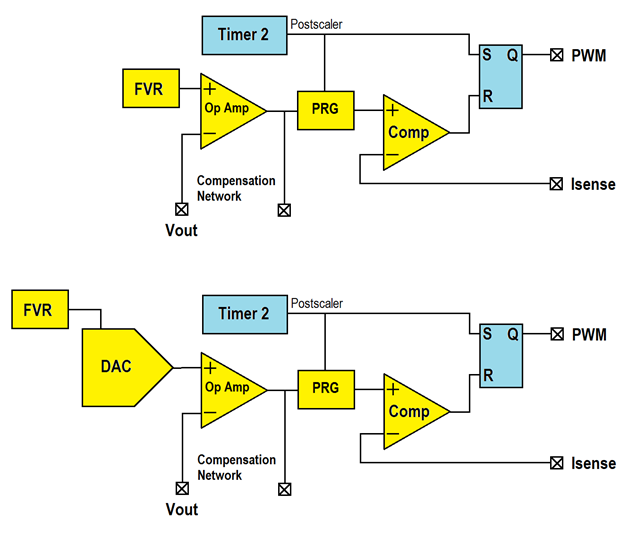
Fig. 13. Adding a PRG module to a PWM controller to eliminate feedback loop instability. Fixed and adjustable output voltage options.
Microchip controllers for power converters like component CIPs have a programmable ramp generator (PRG or Slope Compensation). Add tags