Transistor amplifier practical example work
In amplification mode, the transistor amplifier operates in receiver circuits and audio frequency amplifiers (USF and ULF). During operation, small currents are used in the base circuit, which control large currents in the collector. This is the difference between the amplification mode and the switching mode, which only opens or closes the transistor depending on Ub on the base.
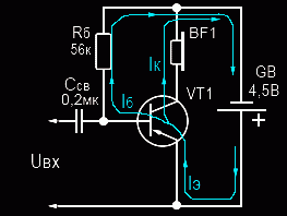
As an experience for a novice radio amateur, we will assemble the simplest transistor amplifier, in accordance with the proposed circuit and drawing.

To the collector VT1 connect a high-impedance telephone BF2, between the base and the minus of the power supply we connect a resistance Rb, and the decoupling capacitance of the capacitor C St..
Of course, we won’t get a strong amplification of the sound signal from such a circuit, but we can hear the sound on the phone BF1 It’s still possible, because we have assembled your first amplifier stage.
An amplification stage is a transistor circuit with resistors, capacitors and other radio components that provide the latter with operating conditions as a transistor amplifier. In addition, we will immediately say that the amplification stages can be connected to each other and obtain multi-stage amplification devices.
When a power source is connected to the circuit, a small negative voltage of about 0.1 - 0.2 V, called bias voltage, goes to the base of the transistor through resistance Rb. It slightly opens the transistor, i.e. reduces the height of the potential barriers, and a small current begins to flow through the junctions of the semiconductor device, which keeps the amplifier in standby mode, from which it can instantly exit as soon as an input signal appears at the input.
Without the presence of bias voltage, the emitter junction will be blocked and, like a diode, will not pass the positive half-cycles of the input voltage, and the amplified signal will be distorted.
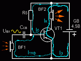
If you connect another telephone to the input of the amplifier and use it as a microphone, then it will convert the sound vibrations arising on its membrane into an alternating voltage in the audio range, which will flow through the capacitance CSV to the base of the transistor.
The capacitor CSV is the connecting component between the phone and the base. It perfectly passes the AF voltage, but creates a serious obstacle to the direct current flowing from the base circuit to the phone. In addition, the phone has an internal resistance of about 1600 Ohms, so without this capacitor capacity, the base would be connected to the emitter through internal resistance and there would be no amplification.
Now, if you start talking into a telephone microphone, then oscillations of the telephone current Itlf will appear in the emitter circuit, which will control the large current arising in the collector, and we will hear these amplified oscillations, converted by the second telephone into ordinary sound.
The process of signal amplification can be represented as follows. When there is no input signal voltage Uin, insignificant currents flow in the base and collector circuits (straight sections of the diagram a, b, c), specified by the applied voltage of the power supply, the bias voltage and the amplification characteristics of the bipolar transistor.
As soon as an input signal arrives at the base (the right side of diagram a), then depending on it, the currents in the circuits of the three-terminal semiconductor device will begin to change (the right side of diagram b, c).
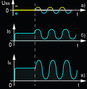
In the negative half-wave of the signal, when Uin and the power supply voltage are summed at the base, the currents flowing through the transistor increase.
With a positive wave, the negative voltage at the base decreases, as do the flowing currents. This is how a transistor amplifier works.
If you connect not a telephone but a resistor to the output, then the voltage of the alternating component of the amplified signal that appears on it can be connected to the input circuit of the second stage for additional amplification. One device is capable of amplifying the signal 30 - 50 times.
VTs of the opposite n-p-n structure work on the same principle. But for them, the polarity of the power supply must be reversed.
For an amplifier transistor to operate, a constant bias voltage must be supplied to its base, relative to the emitter, along with the input signal voltage, which opens the semiconductor device.
For germanium VTs, the opening voltage should be no more than 0.2 volts, and for silicon ones 0.7 volts. The only time bias voltage is not applied to the base is when the emitter junction of the transistor is used to detect a signal, but we will talk about this later.
The transistor amplifier, despite its long history, remains a favorite subject of research for both beginners and seasoned radio amateurs. And this is understandable. He is indispensable integral part the most popular amateur radio devices: radios and low (audio) frequency amplifiers. We will look at how simple transistor amplifiers are built.
Amplifier frequency response
In any television or radio receiver, in every music center or sound amplifier you can find transistor sound amplifiers (low frequency - LF). The difference between transistor audio amplifiers and other types lies in their frequency characteristics.
A transistor-based audio amplifier has a uniform frequency response in the frequency band from 15 Hz to 20 kHz. This means that the amplifier converts (amplify) all input signals with a frequency within this range approximately equally. The figure below shows the ideal frequency response curve for an audio amplifier in the coordinates “amplifier gain Ku - input signal frequency.”
This curve is almost flat from 15 Hz to 20 kHz. This means that such an amplifier should be used specifically for input signals with frequencies between 15 Hz and 20 kHz. For input signals with frequencies above 20 kHz or below 15 Hz, its efficiency and performance degrade quickly.
The type of frequency response of the amplifier is determined by the electrical radio elements (ERE) of its circuit, and primarily by the transistors themselves. A transistor-based audio amplifier is usually assembled using so-called low- and mid-frequency transistors with a total input signal bandwidth from tens and hundreds of Hz to 30 kHz.
Amplifier operating class
As is known, depending on the degree of continuity of current flow throughout its period through a transistor amplification stage (amplifier), the following classes of its operation are distinguished: “A”, “B”, “AB”, “C”, “D”.
In operating class, current “A” flows through the cascade for 100% of the input signal period. The operation of the cascade in this class is illustrated by the following figure.
In the operating class of the amplifier stage "AB", current flows through it for more than 50%, but less than 100% of the input signal period (see figure below). 
In the "B" stage operation class, the current flows through it for exactly 50% of the input signal period, as illustrated in the figure. 
Finally, in class C stage operation, current flows through it for less than 50% of the input signal period.
Low-frequency amplifier using transistors: distortion in the main classes of operation
In the working area, a class “A” transistor amplifier has a low level of nonlinear distortion. But if the signal has pulsed voltage surges, leading to saturation of the transistors, then higher harmonics (up to the 11th) appear around each “standard” harmonic of the output signal. This causes the phenomenon of so-called transistor, or metallic, sound.
If the transistors have an unstabilized power supply, then their output signals are amplitude modulated near the network frequency. This leads to a harsh sound at the left end of the frequency response. Various methods of voltage stabilization make the amplifier design more complex.
The typical efficiency of a single-ended class A amplifier does not exceed 20% due to constant open transistor and continuous flow of the direct current component. You can make a class A amplifier push-pull, the efficiency will increase slightly, but the half-waves of the signal will become more asymmetrical. Transferring a cascade from operating class “A” to operating class “AB” quadruples nonlinear distortions, although the efficiency of its circuit increases.
In class “AB” and “B” amplifiers, distortion increases as the signal level decreases. One involuntarily wants to turn up such an amplifier louder to fully experience the power and dynamics of the music, but often this does not help much.
Intermediate grades of work
Work class "A" has a variation - class "A+". In this case, the low-voltage input transistors of an amplifier of this class operate in class “A”, and the high-voltage output transistors of the amplifier, when their input signals exceed a certain level, go into classes “B” or “AB”. The efficiency of such cascades is better than in pure class “A”, and nonlinear distortions are less (up to 0.003%). However, they also have a “metallic” sound due to the presence of higher harmonics in the output signal.
In amplifiers of another class - "AA" the degree of nonlinear distortion is even lower - about 0.0005%, but higher harmonics are also present.
Return to the Class A transistor amplifier?
Today, many experts in the field of high-quality sound reproduction advocate a return to tube amplifiers, since the level of nonlinear distortions and higher harmonics they introduce into the output signal is obviously lower than that of transistors. However, these advantages are largely offset by the need for a matching transformer between the high-impedance tube output stage and the low-impedance sound speakers. However, a simple transistor amplifier can be made with a transformer output, as will be shown below.
There is also a point of view that the ultimate sound quality can only be provided by a hybrid tube-transistor amplifier, all stages of which are single-ended, not covered and operate in class “A”. That is, such a power repeater is an amplifier with one transistor. Its circuit can have a maximum achievable efficiency (in class “A”) of no more than 50%. But neither the power nor the efficiency of the amplifier are indicators of the quality of sound reproduction. In this case, the quality and linearity of the characteristics of all ERE in the circuit acquire special importance.
Since single-ended circuits are gaining this perspective, we will look at their possible variations below.
Single-ended amplifier with one transistor
Its circuit, made with a common emitter and R-C connections for input and output signals for operation in class “A”, is shown in the figure below. 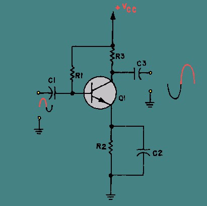
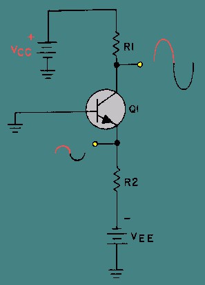
It shows transistor Q1 of the n-p-n structure. Its collector is connected to the positive terminal +Vcc through current-limiting resistor R3, and the emitter is connected to -Vcc. Transistor amplifier p-n-p structures will have the same circuit, but the power supply pins will change places.
C1 is a decoupling capacitor by which the AC input signal source is separated from the DC voltage source Vcc. In this case, C1 does not prevent the passage of alternating input current through the base-emitter junction of transistor Q1. Resistors R1 and R2, together with the resistance of the E - B junction, form Vcc to select the operating point of transistor Q1 in static mode. A typical value for this circuit is R2 = 1 kOhm, and the position of the operating point is Vcc/2. R3 is a load resistor of the collector circuit and serves to create an alternating voltage output signal on the collector.
Let us assume that Vcc = 20 V, R2 = 1 kOhm, and the current gain h = 150. We select the voltage at the emitter Ve = 9 V, and the voltage drop across the “E - B” junction is taken equal to Vbe = 0.7 V. This value corresponds to the so-called silicon transistor. If we were considering an amplifier based on germanium transistors, then the voltage drop across the open junction “E - B” would be equal to Vbe = 0.3 V.
Emitter current approximately equal to collector current
Ie = 9 V/1 kOhm = 9 mA ≈ Ic.
Base current Ib = Ic/h = 9 mA/150 = 60 µA.
Voltage drop across resistor R1
V(R1) = Vcc - Vb = Vcc - (Vbe + Ve) = 20 V - 9.7 V = 10.3 V,
R1 = V(R1)/Ib = 10.3 V/60 µA = 172 kOhm.
C2 is needed to create a circuit for passing the alternating component of the emitter current (actually the collector current). If it were not there, then resistor R2 would greatly limit the variable component, so that the amplifier in question would be bipolar transistor would have low current gain.
In our calculations, we assumed that Ic = Ib h, where Ib is the base current flowing into it from the emitter and arising when a bias voltage is applied to the base. However, a leakage current from the collector Icb0 always flows through the base (both with and without bias). Therefore, the real collector current is equal to Ic = Ib h + Icb0 h, i.e. The leakage current in a circuit with OE is amplified by 150 times. If we were considering an amplifier based on germanium transistors, then this circumstance would need to be taken into account in the calculations. The fact is that germanium transistors have a significant Icb0 of the order of several μA. For silicon, it is three orders of magnitude smaller (about several nA), so it is usually neglected in calculations.
Single-ended amplifier with MOS transistor
Like any amplifier field effect transistors, the circuit under consideration has its analogue among amplifiers on Therefore, let us consider an analogue of the previous circuit with a common emitter. It is made with a common source and R-C connections for input and output signals for operation in class “A” and is shown in the figure below. 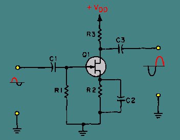
Here C1 is the same decoupling capacitor, through which the AC input signal source is separated from the DC voltage source Vdd. As you know, any amplifier based on field-effect transistors must have the gate potential of its MOS transistors lower than the potentials of their sources. In this circuit, the gate is grounded by resistor R1, which usually has a high resistance (from 100 kOhm to 1 Mohm) so that it does not shunt the input signal. There is practically no current passing through R1, so the gate potential in the absence of an input signal is equal to the ground potential. The source potential is higher than the ground potential due to the voltage drop across resistor R2. Thus, the gate potential is lower than the source potential, which is necessary for normal operation of Q1. Capacitor C2 and resistor R3 have the same purpose as in the previous circuit. Since this is a common source circuit, the input and output signals are 180° out of phase.
Amplifier with transformer output
The third single-stage simple transistor amplifier, shown in the figure below, is also made according to a common-emitter circuit for operation in class "A", but it is connected to a low-impedance speaker through a matching transformer. 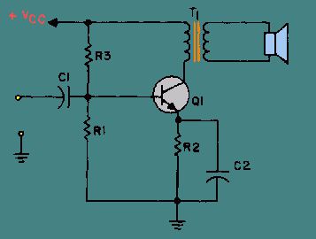
The primary winding of transformer T1 loads the collector circuit of transistor Q1 and develops the output signal. T1 transmits the output signal to the speaker and matches the transistor's output impedance to the low (on the order of a few ohms) impedance of the speaker.
The voltage divider of the collector power supply Vcc, assembled on resistors R1 and R3, ensures the selection of the operating point of transistor Q1 (supplying a bias voltage to its base). The purpose of the remaining elements of the amplifier is the same as in the previous circuits.
Push-pull audio amplifier
A push-pull LF amplifier with two transistors splits the input frequency into two antiphase half-waves, each of which is amplified by its own transistor stage. After performing such amplification, the half-waves are combined into a complete harmonic signal, which is transmitted to the speaker system. Such a transformation of the low-frequency signal (splitting and re-merging), naturally, causes irreversible distortion in it, due to the difference in the frequency and dynamic properties of the two transistors of the circuit. These distortions reduce the sound quality at the amplifier output.
Push-pull amplifiers operating in class “A” do not reproduce complex audio signals well enough, since a direct current of increased magnitude continuously flows in their arms. This leads to asymmetry of signal half-waves, phase distortion and ultimately loss of sound intelligibility. When heated, two powerful transistors double the signal distortion in the low and infra-low frequencies. But still, the main advantage of the push-pull circuit is its acceptable efficiency and increased output power.
A push-pull circuit of a power amplifier using transistors is shown in the figure. 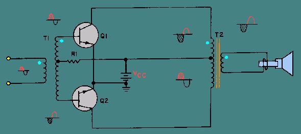
This is an amplifier for operation in class “A”, but class “AB” and even “B” can be used.
Transformerless transistor power amplifier
Transformers, despite the successes in their miniaturization, still remain the most bulky, heaviest and most expensive electronic devices. Therefore, a way was found to eliminate the transformer from the push-pull circuit by implementing it on two powerful complementary transistors different types(n-p-n and p-n-p). Most modern power amplifiers use precisely this principle and are designed to operate in class "B". The circuit of such a power amplifier is shown in the figure below. 
Both of its transistors are connected according to a circuit with a common collector (emitter follower). Therefore, the circuit transfers the input voltage to the output without amplification. If there is no input signal, then both transistors are on the border of the on state, but they are turned off.
When a harmonic signal is applied to the input, its positive half-wave opens TR1, but puts the pnp transistor TR2 completely in cutoff mode. Thus, only the positive half-wave of the amplified current flows through the load. The negative half-wave of the input signal opens only TR2 and closes TR1, so that the negative half-wave of the amplified current is supplied to the load. As a result, a full power-amplified (due to current amplification) sinusoidal signal is released at the load.
Single transistor amplifier
To understand the above, let’s assemble a simple amplifier using transistors with our own hands and figure out how it works.
As a load for a low-power transistor T of type BC107, we will turn on headphones with a resistance of 2-3 kOhm, apply a bias voltage to the base from a high-resistance resistor R* of 1 MOhm, and connect a decoupling electrolytic capacitor C with a capacity of 10 μF to 100 μF into the base circuit T. Power the circuit We will use 4.5 V/0.3 A from the battery. 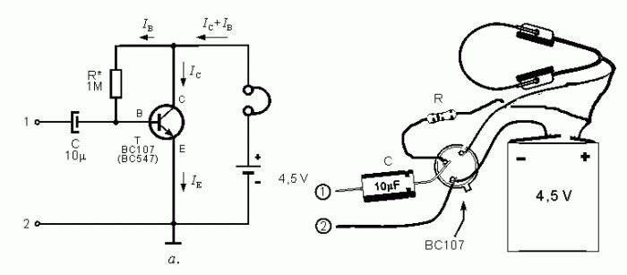
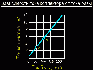
If resistor R* is not connected, then there is neither base current Ib nor collector current Ic. If a resistor is connected, the voltage at the base rises to 0.7 V and a current Ib = 4 μA flows through it. The current gain of the transistor is 250, which gives Ic = 250Ib = 1 mA.
Having assembled a simple transistor amplifier with our own hands, we can now test it. Connect the headphones and place your finger on point 1 of the diagram. You will hear a noise. Your body perceives power supply radiation at a frequency of 50 Hz. The noise you hear from your headphones is this radiation, only amplified by a transistor. Let us explain this process in more detail. A 50 Hz AC voltage is connected to the base of the transistor through capacitor C. The base voltage is now equal to the sum of the DC offset voltage (approximately 0.7 V) coming from resistor R* and the AC finger voltage. As a result, the collector current receives an alternating component with a frequency of 50 Hz. This alternating current is used to shift the speaker membrane back and forth at the same frequency, meaning that we will be able to hear a 50Hz tone at the output.
Listening to a noise level of 50 Hz is not very interesting, so you can connect low-frequency signal sources (CD player or microphone) to points 1 and 2 and hear amplified speech or music.
Sound frequency, without scarce parts.
How to make an amplifier using transistors?
Who doesn’t want to build a good low-frequency power amplifier so that it works “cleanly”, is reliable, and doesn’t take much time to set up. When assembled without errors, it begins to work immediately after supplying voltage to it.
It is only necessary to use resistor R7 to set the output voltage to zero in the absence of a signal at the input and set the initial current of the output transistors VT11, VT12 within 100-150 mA. With a bipolar power supply of ±36 V, the transistor audio power amplifier delivers 50 W to a load with a resistance of 8 Ohms, and 90 W with a load of 4 Ohms.
When the UMZCH operates on a 4-ohm load, the capacity of the smoothing capacitors in the power supply must be at least 20,000 µF for the stereo version or 10,000 µF for the mono version. You should not get carried away with reducing the capacitance of these capacitors, since at high currents in the load, reproduction may deteriorate.
Good results are obtained by using stabilized power supplies. In this case, it is permissible to reduce the capacity of filter capacitors by 1.5 times. In addition, it is not difficult to introduce current protection into a stabilized power supply.
In this case, such protection is not provided, since downtime protection noticeably worsens the quality of sound reproduction, but complex protection significantly increases the number of radio components.
Relay protection circuits are very sensitive to all kinds of interference and voltage surges, so they had to be abandoned. The proposed transistor amplifier is not designed for a stationary audio complex. Carefully assembled, operating on serviceable acoustic systems with a good power reserve, the idle time will last for many years.
As can be seen from Fig. 1, the UMZCH consists of a differential stage VT1, VT2 with a current generator on transistor VI3, a voltage amplifier on transistor VT4 and a buffer stage - current amplifier on transistor VT5. The latter is loaded on a current generator assembled on transistor VF6 and on a symmetrical circuit of a push-pull compound voltage follower on transistors VT7-VT12.
Despite the “traditionality” of this scheme, some “subtleties” are applied to it. The current amplifier VT7-VT12 is somewhat modified compared to conventional circuits. This made it possible to reduce the distortion introduced by the output stage of the UMZCH by several times.
In conventional circuits, due to the presence of base-emitter junction capacitance (this capacitance for high-power transistors can reach hundredths of microfarads), electrical charges accumulate at the bases of output and pre-output transistors, which leads to a delay in transient processes.
In the proposed circuit, the influence of the base-emitter capacitance is reduced several times, which ultimately has a beneficial effect on the fidelity of sound reproduction. The UMZCH is covered by a general environmental protection circuit. Depth of environmental protection alternating current depends on resistors R17 and R16. To reduce the distortion introduced by capacitor C6, it is shunted by a non-electrolytic capacitor C7 with a capacity of 4.7 μF.
Even inexperienced listeners can notice the difference in sound, especially on high frequencies, with and without capacitor C7. To set the zero potential at the output of the UMZCH in the absence of an input signal, use a circuit consisting of elements R3, R6, R7, R14, C3. Through this chain, a small negative bias voltage is applied to transistors VT1 and VT2.
It should be noted that the presence of a VT5 buffer current amplifier makes it possible to reduce distortion by 10-15 roses. Therefore, you should not simplify the circuits by eliminating this cascade. The quiescent current of the output transistors depends on the current of transistor VT6. Therefore, when setting up, if necessary, change the resistance of resistor R18. An increase in the resistance of resistor R18 corresponds to a decrease in the transistor current
VT6 and, conversely, a decrease in R18 causes an increase in the current VT6.
An increase in current through VT6 causes a corresponding increase in the voltage drop across diodes VD1 - VD4, which in turn leads to an increase in the bias voltage of transistors VT7-VT12, while the initial current of output transistors VT11 and VT12 increases. The voltage at the amplifier input at the maximum power it delivers to the load is approximately 1 V.
The harmonic coefficient does not exceed 0.04% over the entire audio frequency range. If you select complementary pairs VT9,VT10 and VT11,VT12 with the same L21e, you can achieve a reduction in Kr to 0.02% in the frequency range up to 16 kHz.
To save good quality For sound reproduction, a pre-amplifier with a tone block must have a low output impedance (several kilo-ohms) and a nonlinear distortion coefficient no more than this UMZCH.
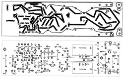
The UMZCH printed circuit board is shown in Fig. 2. It is very convenient to check the amplifier for stability using a generator rectangular pulses, observing the shape of the output signal on the oscilloscope screen. At the same time, the capacitance of capacitor C5 is selected, achieving the least distorted output signal compared to its original form.
If possible, the capacitance C5 is reduced, since the frequency response of the amplifier at high frequencies improves. In fact, the capacitance of the capacitor was reduced to 20 pF when the UMZCH operated but loudspeakers without LC filters, i.e. to full-range loudspeakers. When working with a large reactive load, the capacitance C5 must be increased.
In addition, it is necessary to insert an inductor of several microhenries into the gap in the output wire of the UMZCH. On printed circuit board This coil should be located near the junction point of resistors R26 and R27. When working with a large reactive load, you should also introduce protective diodes (for output transistors) VD7 and VD8 into the UMZCH circuit.
The advantage of an inverting amplifier over a non-inverting amplifier is well known. Since during inverting switching the input signal is supplied to the base of transistor VT2, then input impedance The UMZCH is shunted by resistor R16. In this case, to match the low resistance of the amplifier, for example, with a volume control, it is necessary to turn on a source follower at the UMZCH input.
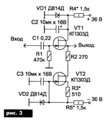
The circuit of such a repeater is shown in Fig. 3 and there is a special place left for it on the printed circuit board. To convert the UMZCH to the inverting version, you must do the following.
- Disconnect capacitors C6, C7 from the common wire and connect the freed leads to the output of the source follower. In this case, the input of the UMZCH will be the input of the repeater.
- Connect the left contact C1 (Fig. 1) to the common wire and connect an electrolytic capacitor in parallel with it in the same way as Sb.
- To avoid clicks and voltage surges at the output of the UMZCH when it is turned on, by selecting resistor R3 (Fig. 3), set the zero potential at the source of transistor VT1.
- The resistances of resistors R4 and R5 are selected in such a way that the zener diodes VD1 and VD2 do not leave the voltage stabilization mode. When switched on invertingly, compared to non-inverting, the amplifier operates somewhat cleaner to the ear.
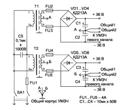
The power supply circuit (PSU) is shown in Fig. 4. In order to reduce distortion, the common wire is divided into two in the skin UMZCH, otherwise distortion increases sharply, “stray” currents appear, which greatly increase the background level in speaker systems. For the same purpose, in the power supply to reduce interference from power transformers, antiphase connection of the primary windings of transformers T1 and T2 is used.
Separate power supply of the UMZCH channels can significantly reduce transient distortion in the channels, especially at low frequencies. The wire diameter of both the secondary and primary windings can also be reduced by 1.4 times compared to one transformer in the UMZCH power supply unit. When using fuses FU2-FU5 (Fig. 4), there is no need for fuses FU1 and FU2 (Fig. 1), but the areas provided for them on the boards are very convenient in case of repairs.
In this case, FU1 and FU2 are replaced with resistors to control currents and prevent failure of transistors VT7-VT12. Transformers T1 and T2 are wound on toroidal magnetic cores, the outer diameter of which is 110 mm, the inner diameter is 65 mm and the height is 23 mm. The primary winding contains 1320 turns of PEV wire - 0.64 mm, the secondary winding is wound double wire PEV - 1.2 mm 162 turns. The screen consists of one layer of PELSHO wire - 0.41 mm.
Transistors KT604, KT611 are suitable for VT5 and VT6. KT618A, KG630. KT940. Instead of transistors KT817 and KT816, the more modern KT850 and KT851 are perfect. You replace transistors VT1 -VT3 with modern KT611A. KT632, 2T638A. The “stumbling block” of the UMZCH is the VT4 transistor; it is recommended to replace it with the modern KT3157A.
This transistor is higher voltage than the KT209M, moreover, it is specially designed for video amplifiers of transistor TVs and has a higher frequency parameter.
The UMZCH works noticeably better with this replacement. The amplifier works great when the power is reduced to ±25 V. It is only necessary to reduce the ratings of R11, R18 (Fig. 1) in order to set the initial currents VT7-VT12 and zero voltage at the output of the UMZCH.
In this case, KT3102A(B) and KT209M can be used in the differential cascade (VT4I can be replaced with KT3107I). Instead of KT818. KT8I9 work better than KT864, KT865 or KT8101, KT8102. It is also proposed to change the circuit for adjusting the initial current of the output transistors by replacing VDI - VD4 and R19 with a slightly different circuit (Fig. 5).
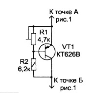
A KT626 type transistor is installed on the heat sink as close as possible to VT12. Transistors VT11 and VT12 are not located on separate heat sinks.
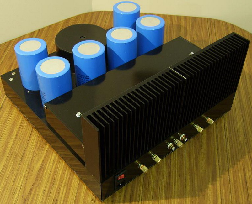
There was a desire to assemble a more powerful Class A amplifier. Having read a sufficient amount of relevant literature and selected the most from what was offered latest version. It was a 30 W amplifier corresponding in its parameters to high-class amplifiers.
I did not intend to make any changes to the existing routing of the original printed circuit boards, however, due to the lack of original power transistors, a more reliable output stage was chosen using 2SA1943 and 2SC5200 transistors. The use of these transistors ultimately made it possible to provide greater output power to the amplifier. Schematic diagram my version of the amplifier below.

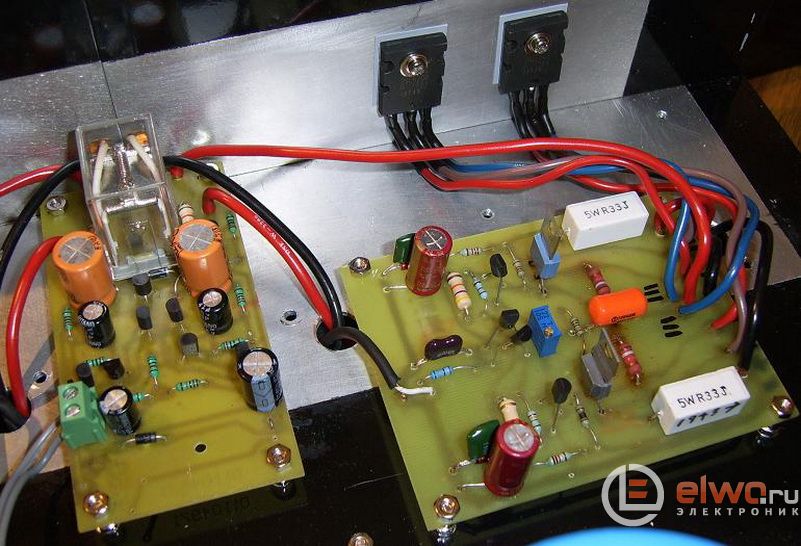
This is an image of boards assembled according to this circuit with Toshiba 2SA1943 and 2SC5200 transistors.
If you look closely, you can see on the printed circuit board along with all the components there are bias resistors, they are 1 W carbon type. It turned out that they are more thermostable. When any high-power amplifier operates, a huge amount of heat is generated, so maintaining a constant rating of the electronic component when heating it is an important condition for the high-quality operation of the device.
The assembled version of the amplifier operates at a current of about 1.6 A and a voltage of 35 V. As a result, 60 W of continuous power is dissipated on the transistors in the output stage. I should note that this is only a third of the power they can handle. Try to imagine how much heat is generated on the radiators when they are heated to 40 degrees.
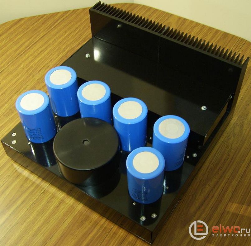
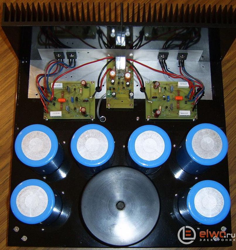
The amplifier case is made by hand from aluminum. Top plate and mounting plate 3mm thick. The radiator consists of two parts, it dimensions are 420 x 180 x 35 mm. Fasteners - screws, mostly with a countersunk head made of of stainless steel and M5 or M3 thread. The number of capacitors was increased to six, their total capacity 220000 uF. Was used for food toroidal transformer power 500 W.
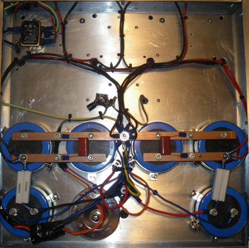
Amplifier power supply
The amplifier device, which has copper busbars of the appropriate design, is clearly visible. Added a small toroid for adjustable feed controlled by DC protection circuit. There is also a high-pass filter in the power supply circuit. For all its simplicity, I must say deceptive simplicity, the board topology of this amplifier and the sound is produced as if without any effort, implying in turn the possibility of its infinite amplification.
Oscillograms of amplifier operation
3 dB roll-off at 208 kHz
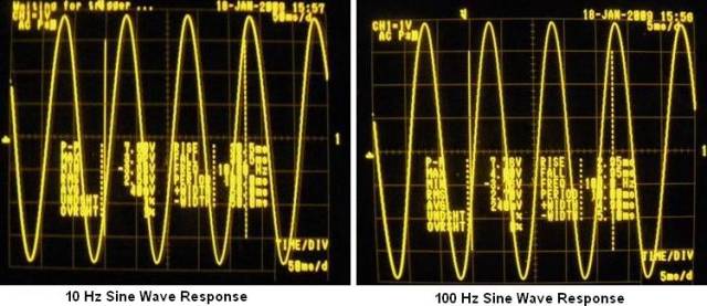
Sine wave 10 Hz and 100 Hz
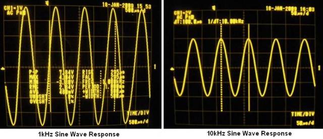
Sine wave 1 kHz and 10 kHz
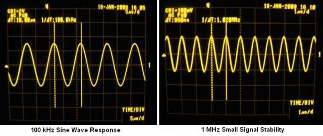
100 kHz and 1 MHz signals
Square wave 10 Hz and 100 Hz

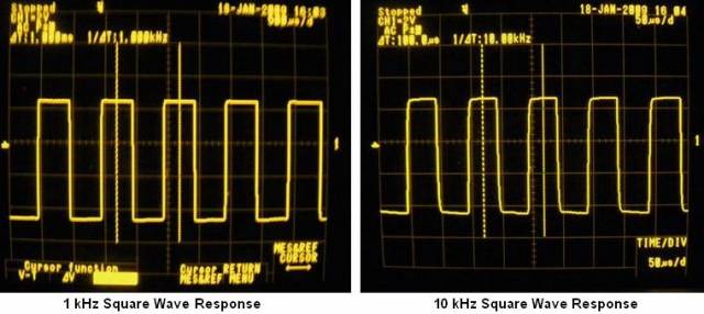
Square wave 1 kHz and 10 kHz
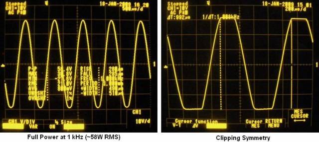
60 W total power, 1 kHz symmetry cutoff
Thus, it becomes clear that a simple and high-quality design of UMZCH is not necessarily made using integrated circuits- only 8 transistors allow you to achieve decent sound with a circuit that can be assembled in half a day.
A low frequency amplifier (LF) is an integral part of most radio devices such as a TV, player, radio and various devices household use. Let's consider two simple circuits two-stage ULF on.
The first version of ULF on transistors
In the first version, the amplifier is built on silicon npn transistors conductivity. The input signal comes through variable resistor R1, which in turn is the load resistance for the signal source circuit. connected to the collector circuit of transistor VT2 of the amplifier.
Setting up the amplifier of the first option comes down to selecting resistances R2 and R4. The resistance value must be selected such that the milliammeter connected to the collector circuit of each transistor shows a current in the region of 0.5...0.8 mA. According to the second scheme, it is also necessary to set the collector current of the second transistor by selecting the resistance of resistor R3.
In the first option, it is possible to use transistors of the KT312 brand, or their foreign analogues, however, it will be necessary to set the correct voltage bias of the transistors by selecting resistances R2, R4. In the second option, in turn, it is possible to use silicon transistors of the KT209, KT361 brands, or foreign analogues. In this case, you can set the operating modes of the transistors by changing the resistance R3.
Instead of headphones, it is possible to connect a high-impedance speaker to the collector circuit of transistor VT2 (both amplifiers). If you need to get more powerful sound amplification, you can assemble an amplifier that provides amplification of up to 15 W.