The described power amplifier is a further development of the design proposed in, in which the anode circuit of the lamp is powered by a transformerless 220 V mains voltage multiplier. I completely agree with the opinion of the author of the mentioned design that the anode transformer is a heavy and unnecessary part in the amplifier. However, do not forget that the amplifier contains high (1200 V) voltage, which is dangerous to life. Do not plug in the amplifier with the cover removed!
Compared to the original, the amplifier circuit has undergone some changes - a filament voltage stabilizer, a transistor bias voltage stabilizer and a bypass circuit control unit have been added.
The input circuit of the amplifier (Fig. 1) is broadband, but to improve its operation there is a resistor rk, made up of three MLT-2 resistors with a resistance of 39 Ohms, it is advisable to replace them with switchable band-pass filters. Resistor r 1 - non-induction (for example, TVO).
In the P-circuit as inductance l 1 a variometer is used (its windings are connected in parallel), which makes it possible to match the amplifier with the antenna inverted vee fed by a symmetrical line through a balun transformer over the entire frequency range from 3 to 14 MHz. In the author's copy of the amplifier, the variable capacitor C8 (the gap between its plates when u a =1200 V must be at least 0.5 mm) was replaced by four capacitors of the K15-U type with a capacity of 33, 68, 150 and 220 pF, which are switched using a flip switch.
The design of the P-circuit may be different, depending on the capabilities of the radio amateur.
Antenna relay K1 is type TKE-54, three groups of contacts K1.1-K1.3 of which are connected in parallel and are used to switch the antenna circuit, and contacts K1.4 are used to turn on the input relay K2. Contacts K2.1 and K2.2 of this relay are also connected in parallel. The applied switching circuit for relay K2 eliminates the possibility of switching contacts K1.1-K1.3 in the presence of a powerful signal at the output of the amplifier.When an RF signal appears at the input of the amplifier, the node" auto TX" on a transistor vt 1 switches the device to transmission mode, which is convenient when working with digital modes of communication. Switch" auto TX" is installed on the front panel of the amplifier.Contrary to classical tradition, the lamp is not locked in receive mode. Firstly, to lock it, a relay with good insulation between the contacts and the winding (at least 2 kV) would be required, and secondly, in the absence of anode current, the cathode will overheat.
To generate the bias voltage, a transistor stabilizer is used vt 3 and vt 4 - a transistor analogue of a zener diode with regulation of the stabilization voltage from 9 to 18 V, which made it possible to adjust the quiescent current of the amplifier (40-50 mA) during operation. When the current through the stabilizer changes from 40 to 300 mA, the stabilization voltage changes by 0.2 V. Transistor vt 3 installed on the radiator.
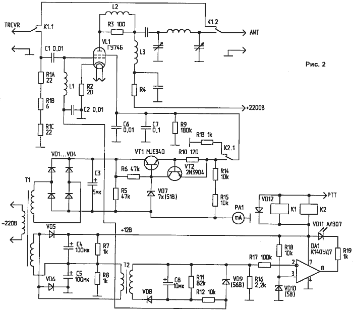
The amplifier power supply circuit is shown in Fig. 2. (corrected)
The filament transformer T1 must havegood insulation between windings. The filament voltage stabilizer is assembled on an integral stabilizer da 1 and transistors vt 1 and vt 2. The stabilizer has a load current limitation of 2.3 A (determined by the resistance of the resistor r 7), which reduces the current overload of the heater when the amplifier is turned on.
The decision to stabilize the lamp filament was made only because of the peculiarities of the local electrical network, the voltage of which “walks” from 180 to 240 V, which means that the filament voltage will vary from 10 to 13 V. If the radio amateur does not have such problems with the network, then a filament stabilizer can not be manufactured, but the 12 V voltage from the winding of the filament transformer should be applied to C13 (Fig. 1).
On transistor vt 3 (Fig. 2) a timer is assembled, which closes the resistor approximately 15 s after turning on the amplifier r 2, limiting the charging current of the electrolytic capacitors of the anode rectifier. Voltage +27 V is used to power relays and indication elements. Transistors vt 2, vt 3 and diode assembly vd 5- vd 8 installed on radiators.
The anode voltage of 1200 V for GI-7B is somewhat low, so it is advisable to make a rectifier according to the circuit shown in Fig. 4 to obtain a voltage of 1800 V. All electrolytic capacitors must have a voltage of at least 350 V. The capacitance of these capacitors is the same and is selected at the rate of 100 μF for every 200 mA of anode current.
The input transformer T1 (Fig. 1) is of the “binoculars” type, assembled from six ferrite rings M2000NM-1 K20x12x6. The transformer windings are wound with three wires folded together, the number of turns is 2. One of the windings, wound with fluoroplastic insulated wire, is the input.
Capacitors C12 and C14 (Fig. 1) are KSO for 250 V. The capacitance of separating capacitors C7 and C10 - type K 15-U can be in the range of 1000-2000 pF. Capacitors must have a threefold voltage reserve and be able to withstand the corresponding reactive power. You cannot save on these capacitors, otherwise trying to use “whatever comes to hand” in these circuits will not end well. Capacitors C5 and C6 are type K15-U or KVI-3.
The manufactured amplifier (case dimensions - 350x310x160 mm) turned out to be safer than any switching computer power supply; the leakage current to ground is 0.05 mA. Since its commissioning, the amplifier has operated ssb -, rtty - and psk -contests, and also functions reliably during everyday work on the air.
With 15 W input power into a 50 ohm equivalent antenna, the amplifier output power at 3,600 MHz is 180 W
RF Power Amplifiers
HF LINEAR TUBE POWER AMPLIFIER TODAY
Part one
Many shortwave operators are convinced that everything is known about tube amplifiers. And even more... Maybe. But the number of low-quality signals on the air is not decreasing. Quite the opposite. And the saddest thing is that all this is happening against the backdrop of an increase in the number of industrial imported transceivers in use, the transmitter parameters of which are quite high and meet the requirements of the FCC (American Federal Communications Commission). However, some of my colleagues on the air, who have come to terms with the fact that you can’t make the FT 1000 “on the knee” and use RAs designed according to the canons of thirty years ago (GU29 + three GU50s), etc., are still confident that according to RA “we ahead of the rest." Let me note that “they are there, abroad,” not only buying, but also constructing RAs that are worthy of attention and repetition.
As you know, KB power amplifiers use circuits with a common grid (OC) and a common cathode (CC). The output stage with OS is almost a standard for radio amateurs in the CIS. Any lamps are used here - both those specially designed to work in a circuit with OS, and lamps for linear amplification in circuits with OK. Apparently, this can be explained by the following reasons:
- the circuit with OS is theoretically not prone to self-excitation, because the grid is grounded either by HF or galvanically;
- in the circuit with feedback, the linearity is 6 dB higher due to the negative feedback by current;
- RA with OS provide higher energy levels than RA with OK.
Unfortunately, what is good in theory is not always good in practice. When using tetrodes and pentodes with a high slope of the current-voltage characteristic, the third grid or beam-forming plates of which are not connected to the cathode, the RA with OS can self-excite. If installation is unsuccessful, low-quality components (especially capacitors) and poor matching with the transceiver, conditions for phase and amplitude balance are easily created to obtain a classic self-oscillator on HF or VHF using a circuit with OS. In general, matching a transceiver with an RA according to the OS scheme is not as simple as it is sometimes written. Often cited figures, such as 75 ohms for four G811s, are only theoretically correct. The input impedance of the PA with feedback depends on the excitation power, anode current, P-circuit settings, etc. Changing any of these parameters, for example increasing the SWR of the antenna at the edge of the range, causes mismatch at the input of the stage. But that's not all. If a tuned circuit is not used at the input of the PA with OS (and this is a common occurrence in homemade amplifiers), then the excitation voltage becomes asymmetrical, because The current from the exciter flows only during the negative half-cycles of the input voltage, and this increases the level of distortion. Thus, it is possible that the above factors will negate the advantages of the OS scheme. But, nevertheless, RA with OS are popular. Why?
In my opinion, due to excellent energy performance: when it is necessary to “pump up power”, there is no price for a circuit with OS. In this case, the linearity of the amplifier is the last thing people think about, referring to what is firmly understood - “the distortions introduced by the cascade depend little on the choice of the operating point on the characteristic.” For example, a GU74B lamp designed for linear amplification of single-sideband signals in a typical connection in a circuit with OK should have a quiescent current of about 200 mA, and it is unlikely that it will be possible to obtain an output power of more than 750 W (at Ua = 2500 V) without risking the longevity of the lamp, t .To. the power dissipation at the anode will be limiting. It’s another matter if the GU74B is turned on with the OS - the quiescent current can be set to less than 50 mA, and an output power of 1 kW can be obtained. It was not possible to find information about measuring the linearity of such RAs, and arguments like “many QSOs were conducted on this amplifier, and correspondents invariably noted high quality signal" - are subjective, therefore, unconvincing. Power of more than 1 kW in the above example is provided by the popular industrial ALPHA/POWER ETO 91B, using a pair of GU74B lamps with OK in the operating mode recommended by the manufacturer with known intermodulation characteristics. Apparently, the developers of this amplifier were are concerned not only with economic considerations (another lamp increases the cost and complicates the design), but also with the compliance of the PA parameters with the standards and requirements of the FCC.
The advantage of RA with OS is the absence of the need to stabilize the voltages of the screen and control grids. This is true only for a circuit in which the specified grids are directly connected to a common wire. Such inclusion of modern tetrodes can hardly be considered correct - not only is there no data on the linearity of the cascade in this mode, but also the power dissipation on the grids, as a rule, exceeds the permissible limit. The excitation power for such a circuit is about 100 W, and this causes increased heating of the transceiver, for example, during intensive work on a general call. In addition, with a long connecting cable, it is necessary to use a switched P-circuit at the amplifier input in order to avoid high SWR values and related problems.
The disadvantages of circuits with OK include the need to stabilize the voltages of the screen and control grids; however, in modern tetrodes in AB1 mode, the power consumed by these circuits is small (20...40 W), and the voltage stabilizers on currently available high-voltage transistors are quite simple. If the power transformer does not have the necessary voltages, you can use suitable low-power transformers by connecting them the other way around - with the secondary winding to a filament voltage of 6.3 or 12.6 V. Another disadvantage of the OK circuit is the high power dissipation at the anode during transmission pauses. One of possible ways its reduction is shown in Fig. 1 (simplified diagram from ). 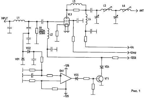
The excitation voltage is supplied through a capacitive divider to the full-wave rectifier VD1, VD2 and then to the comparator DA1. Triggering of the comparator transfers the lamp from the closed state to the operating mode. During transmission pauses, there is no excitation voltage, the lamp is locked, and the power dissipated at the anode is negligible.
In my opinion, RA with OS can be used on KB with outdated lamps - to reduce the cost of the design, or with lamps specially designed to work in such a connection. The use of a tuned LC circuit of low quality factor or a P-circuit at the input is mandatory. This is especially true for transceivers with wideband transistor output stages, the normal operation of which is possible only with a matched load. Of course, if the transceiver output stage has a customizable P-circuit or antenna tuner, and the length connecting cable does not exceed 1.5 m (i.e., it represents a capacitance for the frequency range used), such a circuit can be considered as an input for the PA. But in any case, the use of a P-circuit at the RA input significantly reduces the likelihood of self-excitation on VHF. By the way, this is exactly how the vast majority of PAs with the OS described in foreign literature and produced by industry for shortwave frequencies. For radio amateurs who are planning to create an RA with a power of 500 W or more, it is recommended to use lamps specially designed for linear amplification of radio frequency signals in a circuit with OK. This recommendation becomes especially relevant when using expensive “branded” transceivers - in RA with OS, during self-excitation, there is significant power of RF or microwave oscillations at the input, which can lead to failure of either the output stage or the input circuits of the transceiver (depending on switching of the RX - TX circuit at the moment of self-excitation). Alas, this is not the author’s fantasy, but real cases from practice.
And one more problem cannot be ignored when considering lamp RAs - with light hand V. Zhalnerauskas and V. Drozdov's schemes for constructing the transmitting part of the transceiver have gained popularity when, after a band-pass filter, linear amplification of the radio frequency signal by transistor stages without intermediate filtering is used to excite a tube amplifier. Structurally, the transceiver is simplified, but the price of such simplicity is an increased content of spurious emissions if such circuits are not carefully configured.
The situation gets even worse when the output power of the transceiver is not enough to “drive”, for example in the case of the GU74B with OK with a wideband input circuit on a 1:4 transformer. The required gain is usually achieved by an additional broadband stage. If a low IF is used, and after a two- or three-loop DFT, the transmitting path has a gain of 40...60 dB in power, and the P-loop is the only selective circuit of this path, then sufficient suppression of spurious emissions is not ensured. The effects can be heard on the amateur bands every day, such as second harmonics almost equal in power to the main signal. Listen, for example, to the 3680...3860 kHz section, and you will almost certainly hear second harmonic signals from SSB stations on the 160-meter range. The RA itself also has a certain nonlinearity, so even when a spectrally pure radio frequency signal is supplied to it, harmonics are inevitably present at the output. A single P-circuit can be recommended for output power up to 1 kW. With higher power, foreign amateur and industrial RAs use P-L circuit, shown in Fig. 1 - its filtration coefficient is twice as high.
Let us now consider circuit solutions that demonstrate a rather demanding approach to the design of RA.
The publication introduces us to the American version of the homemade RA on the GU74B. George T. Daughters, AB6YL, having decided to remake the Dentron MLA2500 industrial amplifier, originally built on triodes according to the OS circuit, opted for the GU74B lamp (American designation - 4СХ800А). For this project, he considered it optimal to use the mode of supplying the excitation signal to the control grid, where the input power is dissipated by a fifty-ohm resistor between the grid and the common wire. This eliminated the need for customized input circuits and easily provided broadband. The low impedance of the control grid circuit helps avoid self-excitation and provides the transceiver's output stage with a stable resistive load with low SWR. In addition, the very popular commercial amplifier ALPHA/POWER 91B with an output power of 1500 W uses a pair of 4CX800A in this connection - this is an already proven circuit!
The amplifier circuit is shown in Fig. 2.
The large input capacitance of the 4CX800A (about 50 pF) requires the use of inductive compensation, especially in high frequency ranges. Wirewound resistor R1B 6 W/6 Ohm provides the necessary inductance and, together with non-inductive R1A and R1C, complements the load resistance to the required 50 Ohm/50 W. According to AB6YL measurements, at frequencies below 35 MHz the input SWR is less than 1.1.
The energy performance of the amplifier can be improved by connecting a non-inductive resistor R2 with a resistance of up to 30 Ohms between the cathode and the common wire. This resistor provides negative feedback, which reduces the quiescent current and slightly improves linearity; the level of fifth-order components decreases by approximately 3 dB.
The parameters of the P-circuit are not given, because Components from Dentron - MLA2500 were used.
The 4СХ800А filament must be turned on at least 2.5 minutes before the excitation and supply voltages are applied.
Specifications for 4СХ800А/ГУ74Б, supplied to the American market, recommend a bias voltage on the control grid of about -56 V with a screen voltage of +350 V. The control grid power supply consists of a low-power transformer T2, connected in reverse - to the secondary winding, used as the primary, A voltage of 6.3 V is supplied from the main transformer T1, which provides about 60 V AC voltage. At the output of the parametric stabilizer VD9, R12 there is a voltage of -56 V. Any control grid current causes nonlinear distortion leading to splatter. The grid current detector is assembled on an operational amplifier DA1, connected according to a comparator circuit. When the grid current exceeds a few milliamps, the voltage drop across R16 increases, causing the comparator to operate and the red LED to glow.
The screen grid is powered by a voltage stabilizer (VT1, VT2, VD7) with protection against excess current consumption. Relay contacts K2 switch the screen grid between the common wire (via R13) in receive mode and +350 V in transmit mode. Resistor R9 prevents voltage surges when switching the relay. The screen grid current is indicated by the PA1 pointer device, because For tetrodes, the screen grid current is a better indicator of resonance and tuning than the anode current. In transmit mode, the anode quiescent current should be 150...200 mA, while the screen grid current is about -5 mA (if a device without a zero in the middle is used, the arrow will move to the left all the way). The amplifier operates in linear mode and does not need ALC (as long as there is no control grid current) with an anode current of 550...600 mA and a screen grid current of approximately 25 mA. If the screen grid current at resonance exceeds 30 mA, it is necessary to increase the connection to the load or reduce the excitation power. When tuning tetrode amplifiers, it must be remembered that the anode current increases with increasing excitation power; screen grid current is maximum at resonance or weak connection with load. When adjusting the amplifier for maximum output power, you should not exceed the parameters specified in the specifications for optimal linearity. The required amplifier excitation power decreases in high frequency ranges. This is explained by the influence of the cathode-heater capacitance, which shunts resistor R2, reducing the environmental impact. This must be kept in mind to avoid over-exciting the amplifier on 15 and 10 meters. (Or use an RF choke in the filament circuit. Ed.)
The amplifier parameters with an input power of about 45 W are given in Table 1. (The output power value seems to be somewhat overestimated. Editor's note.) Before turning off the amplifier after a session, you need to leave it in the standby position for about three minutes - the fan should cool the lamp.
Table 1
Anode voltage 2200 V
Anode quiescent current 170 mA
Maximum anode current 550 mA
Screen grid current maximum 25 mA 0
Power dissipation at the anode without signal 370 W
Power supplied 1200 W
Output power 750W
Part two
The desire to provide reliable and durable performance of a highly linear power amplifier was clearly demonstrated by Mark Mandelkern, KN5S. Schematic diagrams amplifier and auxiliary circuits are shown in Fig. 3...8. 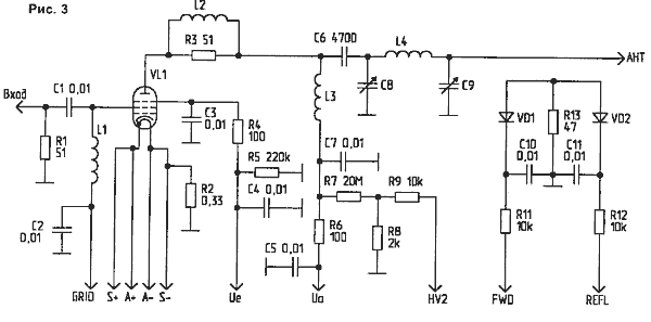
Do not be surprised by the abundance of semiconductor devices - their use is justified and deserves attention, especially the use of protection circuits. (However, it cannot be said that all of them are absolutely necessary. Ed.)
When designing the RA, the following goals were pursued:
- power supply of the lamp heater from a stabilized DC source; use of automatic heating and cooling timers;
- measurement of all parameters, including anode current and voltage, without inconvenient switching;
- the presence of stabilized sources of bias and screen voltage, allowing voltage adjustment within a wide range;
- ensuring operability under significant fluctuations in network voltage (this is especially true when working in the field using an electric current generator).
The power source for the heater of powerful generator lamps is rarely given due attention, but it largely determines the longevity of the lamp and the stability of the output power. Warming up of the heater should occur gradually, avoiding current surges through the cold filament. In transmission mode, when intense electron emission occurs, it is very important to ensure a constant filament voltage and, accordingly, a constant cathode temperature. These are the main reasons for using a stabilized power source with a current limiter for incandescent lamps, which eliminates the current surge at the moment of switching on.
The power supply diagram is shown in Fig.4. The output voltages allow the following adjustment ranges: from 5.5 to 6 V (filament), from 200 to 350 V (screen grid) and from -25 to -125 V (control grid).
The filament voltage stabilizer uses the popular LN723 microcircuit in a typical connection. The significant filament current of the 4CX1000 tetrode (about 9 A) and the connection of the cathode and heater inside the lamp required separate large-section conductors for the high-current circuit (A- and A+); Through the S- and S+ circuit, the output voltage is supplied to the stabilizer comparison circuit. It is best to solder the FU1 10 A fuse rather than use a fuse holder.
The heater control circuit is shown in Fig.5. The circuit eliminates the use of the amplifier during warm-up and protects the heater from increased voltage if the stabilizer malfunctions. Protection is provided by turning off the heater using relay K2 (Fig. 4). In addition, the air flow sensor through the lamp SA2 (Fig. 4) monitors the performance of the fan. If there is no air flow, this will also cause relay K2 and the filament voltage regulator to turn off.
The warm-up timer (DA3 in Fig. 5) is set to five minutes. According to the specifications, three minutes is enough, but longer heating will extend the life of the lamp. The timer starts only after voltage appears on the heater. This is determined by the comparator DA2.2 connected to point S+. So, for example, if a fuse is blown, the timer will not start until you replace the fuse. When the voltage is exceeded (for example, when the control transistor VT1 breaks down), the trigger on DA2.3 is activated and the transistor VT2 closes, disconnecting the voltage from the winding of relay K2 (point HR in Fig. 5). Capacitor SZ ensures the initial setting of the trigger and, accordingly, the opening of transistor VT2 when the supply voltage is applied.
Along with the warm-up timer, the amplifier needs a timer for the tube to cool down before turning off (DA4). When the amplifier is turned off, the +12 V circuit discharges faster than the +24 V circuit (which has a minimum load in receive mode). A voltage of +24 V appears at the DA2.1 output and the cooling timer starts. After startup, DA4 is present at pin 7 low level voltage, leading to the operation of relay K1 (Fig. 4), through the contacts of which the operation of the stabilizers +12/-12 V and +24 V is ensured. After approximately three minutes, a high level appears at pin 7, relay K1 returns to its original state, and the amplifier finally de-energized. The +24 RLY circuit eliminates the operation of the cooling timer if for some reason the amplifier was turned off and immediately turned on. For example, the passage of radio waves ends and the range seems dead - you turn off the amplifier. Suddenly an interesting correspondent appears - the power switch is again in the ON position! When entering transmit mode, the +24RLY voltage forces DA2.1 to a low state and resets the cooling timer.
As in the case of filament voltage, the screen grid voltage stabilizer rarely receives attention when designing a PA. But in vain... Powerful tetrodes, due to the phenomenon of secondary emission, have a negative screen grid current, so the power source of this circuit must not only supply current to the load, but also consume it when the direction changes. Sequential Circuits stabilizers do not provide this, and when a negative screen grid current appears, the series stabilizer transistor may fail. Having lost several high-voltage transistors when setting up the amplifier, radio amateurs come to the decision to install a powerful resistor with a resistance of 5...15 kOhm between the screen grid and the common wire, resigning themselves to useless power dissipation. The use of a parallel voltage stabilizer, which can not only supply, but also receive current, allows for trouble-free operation, but it is advisable to use overcurrent protection.
The screen grid voltage stabilizer is assembled using transistors VT3, VT4 (Fig. 4). Instead of VT3 type 2N2222A, you can use a high-voltage one, excluding the parametric stabilizer R6, VD5, but in this case the stabilization coefficient may deteriorate, because high-voltage transistors have low gain. The output voltage is determined by the sum of the stabilization voltage VD11 and the voltage at the base-emitter junctions of transistors VT3, VT4 (15+0.6+0.6=16.2 V), multiplied by the coefficient determined by the voltage divider R11,R12,R13 (12. ..20) at the output of the stabilizer.
The shunt transistor is mounted directly on an aluminum plate measuring 70x100x5 mm, which, in turn, is mounted on the side wall using ceramic insulators. Resistor R7 limits the peak current through shunt transistor VT4 to about 100 mA.
RECEPTION-TRANSMITTING Scheme (Fig.6) checks six signals: the presence of air flow through the lamp (+12H), the state of the OPERATE-STANDBY switch, the completion of filament heating, the presence of anode voltage, the presence of bias voltage and the state of the overload protection circuit. The reception-transmission switching circuit provides a delay in the operation of the short-circuit relay of 50 ms (Fig. 4) when switching to transmission and a delay in turning off the coaxial relay of 15 ms when switching to reception. If used vacuum relays, the relay timing can be easily changed for full QSK.
The operational amplifiers of the receive-transmit switching circuit in Fig. 6 use very simple R-C circuits to obtain switching delay. In transmit mode, there is a voltage of about +11 V at the output of DA1.4, which provides a quick charge of capacitor C4 through the diode VD8 of the Kant antenna switching coaxial relay circuit. Capacitor C5 of the screen grid power relay circuit is charged through resistor R26, so the screen relay operates later. When switching to receive mode, a voltage of about -11 V appears at the DA1.4 output, and the reverse process occurs. The KEY input allows you to reduce power dissipation at the anode during transmission pauses and avoid changing the shape of the CW signal sent when working with PA, but for this it is necessary that the transceiver has an appropriate output. The overload blocking circuit (Fig. 7) is triggered when the control or screen grid or anode current exceeds 1 mA, -30 mA and 1150 mA, respectively. The screen grid overload protection circuit operates only at negative currents. The positive current limiter of the screen grid is resistor R27 in the voltage stabilizer circuit. Overload protection circuit tripping (Fig.8) causes the TRANSMISSION-RECEIVE circuit to turn off via the OL circuit (Fig. 6), turn on an additional resistor R2 in the control grid bias circuit using the contacts of relay K1, turn on the generator on DA2.4 and flash the red LED VD9 OVERLOAD on the front panel.
Only the DA2 microcircuit is powered from a unipolar +24 V source (Fig. 5). All other op amps use +12/-12 V supply voltage.
On Fig.7 The measurement diagram is shown. Five pointer instruments allow you to measure 10(!) parameters using additional buttons: direct/reflected power in the antenna, control grid current/voltage, anode current/voltage, screen grid current/voltage, filament voltage/current. To read the parameter values indicated through a fraction, you must press the corresponding button. Basic parameters are read immediately; secondary parameters have great importance only for initial setup and for adjustments after lamp replacement. The simplest non-inverting amplifier used here is to measure the anode voltage (DA2.1). Let us assume that the measurement limit should be 5000 V; The divider R7, R8 (Fig. 3) has a division coefficient of 10,000, i.e. 5000 V at point HV2 is 0.5 V. Resistor R9 does not affect the operation of the circuit, since the operational amplifier has a high input impedance. With a supply voltage of +12/-12 V, the maximum output voltage of the amplifier is about +11/-11 V. Let us assume that +10 V of the output voltage of the operational amplifier corresponds to the full deflection of the meter needle when using a 10 kOhm resistor R22 and a 1 mA device. The required gain (10/0.5) is 20. Having chosen R15 = 10k0m, we find that the feedback resistor should have a resistance of 190 kOhm. The specified resistor is composed of a trimming resistor R20 with a resistance of approximately half the nominal value and a constant resistor R19, selected from a number of standard values.
The anode current measurement circuit is similar. A voltage proportional to the anode current is removed from the negative feedback resistor R2 in the cathode circuit (Fig. 3). Capacitor C2 provides damping of the readings of the measuring device ONCE during SSB operation.
Screen voltage is measured in a similar way. The values of the resistors that determine the gain of the forward and reverse power measurement circuits depend on the design of the directional coupler.
The screen grid current measurement circuit is implemented somewhat differently. It was indicated above that the screen grid current can have both negative and positive values, i.e. a measuring device with a zero in the middle is required. The circuit is implemented on a DA2.3 operational amplifier and has a measurement range of -50...0...50 mA, using a conventional device with a zero on the left for indication.
At 50 mA positive screen grid current, the voltage drop across resistor R23 (Fig. 4) is -5V at point -E2. Thus, a gain of -1 is required from the op amp to produce the required +5V output voltage to deflect the needle by half scale. When R23=10 kOhm, the feedback resistor should have a nominal value of 10 kOhm; tuning resistors R32 and constant resistors R30 are used. To shift the instrument needle to the middle of the scale at a supply voltage of -12 V, a gain of +5/-12=-0.417 is required. The exact value of the gain and, accordingly, the zero of the scale is set by trimming resistor R25.
Operational amplifiers DA2.2, DA2.4 have an extended filament voltage measurement scale. The differential amplifier DA2.2 converts the filament voltage to unipolar, because point S is not directly connected to the common wire. The DA2.4 summing amplifier implements an extended measurement scale - from 5.0 to 6.0 V. In fact, it is a voltmeter with a measurement limit of 1 V, biased to the initial value of 5 V.
In rectifier circuits, the diodes used must be designed for the appropriate current, the rest - any pulse silicon diodes. With the exception of high-voltage transistors, any low-power corresponding structure can be used. Operational amplifiers - LM324 or similar. Measuring instruments- PA1...PA5 with a total deviation current of 1 mA.
The above schemes certainly complicate RA. But for reliable everyday work on air and in competitions, it’s worth spending the extra effort to create a truly high-quality device. If there are more clean and loud signals on the bands, then all radio amateurs will benefit. For QRO without QRM! I express my gratitude to I. Goncharenko (EU1TT), whose advice and comments were of great help when working on the article.
Literature
1. Bunimovich S., Yailenko L. Amateur single-sideband radio communication technology. - Moscow, DOSAAF, 1970.
2. Radio, 1986, N4, P.20.
3. Drozdov V. Amateur KB transceivers. - Moscow, Radio and Communications, 1988.
4. QST ON CD-ROM, 1996, N5.
5. http: //www.svetlana.com/.
6. QEX ON CD-ROM, 1996, N5.
7. QEX ON CD-ROM, 1996, N11.
8. Radio amateur. KB and UKV, 1998, N2, P.24.
9. Radio Amateur, 1992, N6, P.38.
10. ALPHA/POWER ETO 91B User's Manual.
G.LIVER (EW1EA) "HF and VHF" No. 9 1998
I present to your attention a power amplifier for a HF transceiver on field effect transistors IRF510.
With an input power of about 1 watt, the output is easily 100-150 watts.
I immediately apologize for the quality of the diagram.
The amplifier is two-stage. Both stages are made on popular and cheap key mosfets, which distinguishes this design from many others. The first stage is single-ended. Input matching with a 50 Ohm signal source was not the best, but in a simple way- using a 51 Ohm resistor R4 at the input. The load of the cascade is the primary winding of the interstage matching transformer. The cascade is covered by a negative feedback circuit to equalize the frequency response. L1, included in this circuit, reduces the OOS in the area higher frequencies and thereby increases the gain. The same goal is pursued by installing C1 in parallel with the resistor at the source of the transistor. The second cascade is push-pull. In order to minimize harmonics, separate displacement of the cascade arms is applied. Each shoulder is also covered by an OOS chain. The load of the cascade is transformer Tr3, and matching and transition to an asymmetric load is provided by Tr2. The bias of each stage and, accordingly, the quiescent current are set separately using trimming resistors. Voltage is supplied to these resistors through the PTT switch on transistor T6. Switching to TX occurs when the PTT point is shorted to ground. Bias voltage stabilized at 5V integral stabilizer. In general, a very simple scheme with good performance characteristics.
Now about the details. All amplifier transistors are IRF510. Others can be used, but with them you can expect an increase in the gain rolloff in the frequency range above 20 MHz, since the input and pass-through capacitances of the IRF-510 transistors are the lowest of the entire line of key mosfets. If you can find MS-1307 transistors, you can count on a significant improvement in the performance of the amplifier in the higher frequencies. But they are expensive... The inductance of chokes Dr1 and Dr2 is not critical - they are wound on rings of 1000NN ferrite with 0.8 wire in one layer until filled. All capacitors are SMD. Capacitors C5, C6 and especially C14, C15 must have sufficient reactive power. If necessary, you can use several capacitors connected in parallel. To ensure high-quality operation of the amplifier, it is necessary Special attention focus on the manufacture of transformers. Tr3 is wound on a 600NN ferrite ring with an outer diameter of 22 mm and contains 2 windings of 7 turns each. It is wound into two wires that are slightly twisted. Wire - PEL-2 0.9.
Tr1 and Tr2 are made according to the classic design of a single-turn SHPT (aka “binoculars”). Tr1 is made on 10 rings (2 columns of 5 each) made of 1000NN ferrite with a diameter of 12 mm. The windings are made of thick MGTF wire. The first contains 5 turns, the second - 2 turns. Good results makes it possible to make windings from several wires of a smaller cross-section connected in parallel. Tr2 is made using ferrite tubes taken from the monitor signal cords. Copper tubes are tightly inserted inside their holes, which form one turn - the primary winding. A secondary winding is wound inside, which contains 4 turns and is made of MGTF wire. (7 wires in parallel). This circuit does not have elements to protect the output stage from high SWR, except for the built-in structural diodes, which effectively protect the transistors from “instantaneous” overvoltages at the drains. Protection against SWR is handled by a separate unit, built on the basis of an SWR meter and reducing the supply voltage when the SWR increases above a certain limit. This diagram is the topic of a separate article. Resistors R1-R4,R7-R9,R17,R10,R11 - type MLT-1.R6 - MLT-2. R13,R12 - MLT-0.5. The rest are SMD 0.25 W.


