What should I put at the input of a stereo amplifier on the TDA1552 chip to control sound? Regular double resistor. What if we have quad switching for 4 channels? Someone suggests - a quad controller :) What if we assembled a home theater with 6 channels? This is where complex and expensive electronic volume controls on specialized chips come into play. And such a unit can exceed the amplifier itself in complexity and price. However, there is a simple way out, how to implement the volume control function with just one transistor. The circuit proposed below from a radio amateur magazine allows one variable resistor to control the volume of several channels at once.
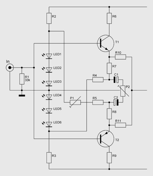
Actually the circuit of the active volume control itself:
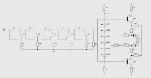
Regulator circuit for four channels with one resistor:
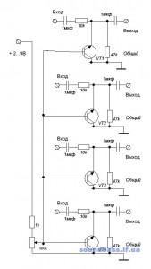
One diagram shows one channel of the volume control, and the other shows 4 channels at once. Naturally, there can be 5 or 10 of them. The essence of the method is that by applying a positive potential to the base of the transistor through a resistor, the transistor opens and bypasses the ULF input - the volume decreases.
A number of experiments were carried out with this scheme. It turned out that the base power can be taken starting from 1.5V. The maximum voltage limit is determined by a 1 kOhm limiting resistor. If we found in the ULF, let’s say 12V, then the resistor must be increased to 30 kOhm, which is safe for the base current. Current consumption of the base circuit in open state- several milliamps. In general, you will choose.
When the transistor is open, a very quiet sound may be heard due to the voltage drop across the silicon crystal. For complete silence, you need to use a germanium transistor of the MP36 - MP38 type.
The capacitors at the input and output of the electronic volume control are non-polar. We install any transistor low-power N-P-N, type KT315, KT3102, S9014, etc. Variable resistor for an electronic regulator with a resistance in the range of 10-100 kOhm. Preferably with a linear characteristic.
When the engine is shorted to ground, all transistors will close and the volume will become maximum. By moving the slider to the power positive, we gradually open the transistors and the sound will begin to subside. Using the resistor that is connected to the power positive, we set the smoothness of the volume change throughout the entire rotation of the resistor. So that it doesn’t happen when after half a turn the volume disappears and we continue turning in vain. Using this electronic volume control, on the one hand, will slightly increase the noise level, but on the other hand, it will reduce interference on the wires, since now there is no need to pull a twice-shielded wire from the preamplifier output to the power amplifier input.
In this part of the article we will talk about aspects of matching the Nikitin volume control with an amplifier.
To obtain the declared parameters, reduce distortion and ensure smooth volume control, the Nikitin regulator must be matched to input impedance amplifier!
Let's look at it in order:
- General issues regulator approval.
- Coordination of the regulator with op-amp circuits and transistors.
- Matching the regulator with tube stages.
1. General approval issues.
To consider the general nuances of matching Nikitin’s volume control with amplifiers, let’s turn to the article “ Distortions that occur in op-amp cascades when regulating the signal level,” author V.A. Svintenok.
I won’t give it in full (those who are interested can easily find it on the Internet). In it, the author, having conducted not entirely correct and incomplete experiments, confirmed known fact that amplifiers in an inverting connection sound better and have less distortion than amplifiers in a non-inverting connection. This feature has long been noticed and tried to explain Douglas Self And Nikolay Sukhov(the author of that very “high fidelity amplifier”). The latter came to the conclusion that such an effect is caused by the fact that in a non-inverting inclusion transition b-e input transistor is outside the common negative circuit feedback, due to which the Miller capacity is not compensated. Accordingly, for an amplifier with field effect transistors at the input, a similar effect is either much weaker or not observed at all.
But Nikitina also took part in the experiments described in the article. Sometimes, however, it is not entirely correct. It’s not clear why it was necessary to take the characteristics of an unloaded regulator??? I repeat once again that in order to ensure the stated parameters (adjustment step, uniformity of adjustment, adjustment range, etc.), the regulator must be matched to load!!!
Note: in this article Nikitina is more often referred to as « ladder type".
So, the most interesting and useful conclusions from the article:
...As was shown above, the non-inverting connection of an op-amp with resistors at the inputs does not allow the maximum potential of most microcircuits to be realized for nonlinear distortion. Inverting switching gives the series best characteristics: less nonlinear distortion, shorter and “softer” distortion spectrum, absence of a “threshold” (a sharp increase in higher harmonics in the spectrum), distortion and spectrum are not affected by the internal resistance of the signal source.
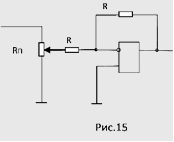
The standard design of a level controller with a buffer follower in an inverting connection is shown in Fig. 15. In practice, this scheme is used quite rarely and this is due to the following. To save input impedance circuits at the resistance value levelRп and the law of change in resistance depending on the angle of rotation of the potentiometer handle is necessary so that the condition is satisfied for the resistors of the circuitR>Rп (3 or more times). To obtain an acceptable input impedance of the circuit, you have to choose fairly high-resistance resistorsR. And this in turn leads to an increased noise level of the circuit.
However, let's consider this circuit as a starting circuit for this type of inclusion.
For the circuit shown in Fig. 15, the maximum distortion will be in the upper position of the potentiometer sliderRп and correspond to the repeater in the inverting connection. Further, as the signal level at the output of the potentiometer decreases, the distortion at the output of the op-amp will begin to decrease proportionally. In this connection, it is sufficient to characterize the behavior of the active element in the regulator by describing it at one point - at the point of observation of maximum distortion.
Table 10 shows harmonic coefficients for input voltages of 2 and 4 volts for an inverter assembled according to the diagram in Fig. 15 with resistor valuesR = 5 kOhm and with the controller transmission coefficient Kp = -1.
Table 10.
|
Table 10 (1) |
||||||||
|
Type ms |
OPA2134 |
AD8620 |
NE5532 |
OP275 |
||||
|
Uin(in) |
||||||||
|
K g7%(5k) |
0,000066 |
0,000035 |
0,000062 |
|||||
|
Table 10 (2) |
||||||||
|
Type ms |
LME49860 |
AD8066 |
AD826 |
J.R.C.2114 |
||||
|
Uin(in) |
||||||||
|
K g7%(5k) |
0,000012 |
0,000032 |
0,000024 |
0,000092 |
0,000039 |
|||
|
Table 10 (3) |
||||||||
|
Type ms |
T.H.S.4062 |
AD8599 |
LT1220 |
AD825 |
||||
|
Uin(in) |
||||||||
|
K g7%(5k) |
||||||||
|
Table 10 (4) |
||||||||
|
Type ms |
LME49710 |
L.M.6171 |
||||||
|
Uin(in) |
||||||||
|
K g7%(5k) |
0,000013 |
5,2*10 -6 |
||||||
Analyzing the data given in Table 10, you can see that the choice of microcircuits for building signal level regulators with low distortion is much wider.
The best chips in this inclusionLME49860, LME49710 AndAD8066. In addition to excellent nonlinear distortion characteristics, they also have an excellent distortion spectrum: 2–3 harmonics at an input voltage of four volts.
Excellent characteristics andJRC2114, OP275 AndNE5532. The spectra of the first two microcircuits contain 4–5 harmonics at an input voltage of 4 volts, butNE5532 is long, with a dip. It is best used with an input voltage of less than four volts.
Good spectra (four harmonics) at an input voltage of 4 volts andAD826, THS4062, LT1220. MicrocircuitsOPA2134, AD5599 AndAD8620 It is better to use an input voltage of two volts or less. ULM6171 V inverting when switched on, the distortion is significantly higher, and the nature and behavior of the spectrum from the supply voltage is the same as in a non-inverting switch.
As mentioned above, in practice, to realize the high potential for distortion in of this type regulator is problematic due to the inherent disadvantages of this inclusion. So, to obtain an input resistance close to 10 kOhm, it is necessary to select fairly high-resistance resistors (more than 30 kOhm) in the inverter circuit, which will lead to a significant increase in the noise of the regulator and will reduce the number of microcircuits capable of operating at a sufficiently high quality level in this connection. To a large extent, these problems can be solved if a “ladder” type signal level regulator is used in this connection...
...to do this, it is necessary to disconnect the load resistor of the regulator from the common wire and connect it to the inverting input of the op-amp, as shown in Fig. 16.
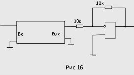
All the advantages of this regulator are preserved in this connection. With a controller gain of 0 dB, the circuit is an inverter with unity gain and an input impedance of 10 kOhm. The maximum distortion of such a regulator corresponds to the maximum signal at the inverter input and will correspond to the data values given in Table 10. At the regulator input, you can turn onRC chain for restraint high frequencies without fear of increasing nonlinear distortion. As the voltage decreases, distortion will also decrease, which is a normal and natural property of the regulator in this connection.
The maximum signal attenuation coefficient and frequency response are determined by the maximum attenuation of the regulator and its frequency response
Looking ahead a little, we can say that this is one of the best solutions allowing to obtain the minimum achievable nonlinear distortions with a “soft” and short spectrum. In this connection, distortions are achievable, not exceeding the level of a few hundred thousandths at 4 volts at the input with a monotonic decrease in distortion as the attenuation coefficient of the regulator increases.
The only weak point of the regulator is noise. They will be determined by resistors (equivalent value no more than 6 kOhm) and the inverter noise transmission coefficient (equal to two) ...
It should also be noted that during experiments with non-inverting When the amplifier was turned on, the author detected an increase in distortion with an increase in the mounting capacity of the regulator. Therefore, when assembling the circuit in this version, you should pay attention Special attention elements of the regulator, their location and installation method!
2. Coordination of Nikitin’s volume control with op-amp and transistor circuits.
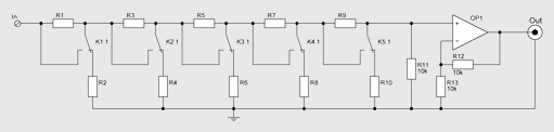
An example of matching Nikitin's volume control with non-inverting amplifier:
click to zoom
Here, the input impedance of the amplifier is determined by the value of resistor R11. To coordinate with the volume control, its nominal value is 10 kOhm. If you need to obtain more gain from the op-amp, you can increase the value of resistor R12.
Let me remind you that this circuit does not fully realize the potential of the operational amplifier (in terms of parameters and sound quality) and the circuit is quite sensitive to the capacity (quality) of the installation. Therefore, it is recommended to use it only in case of emergency.
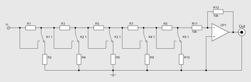
When using an op-amp in inverting inclusion of the above disadvantages are eliminated:
click to zoom
Here, the input impedance of the amplifier is determined by the value of resistor R11. To coordinate with the Nikitin volume control, its value was selected as 10 kOhm.
Attention! In the diagrams shown, the resistor values are indicated to match the Nikitin volume control with the load 10kOhm. If the regulator is designed for a different load (for example, using a table from), the values of the indicated resistors need to change to the relevant ones.
An example of matching a regulator with a real amplifier:
The figure shows the input stage of V. Korol’s modernized power amplifier:
The cascade is made according to a push-pull circuit, and with identical parameters of complementary transistors T1 and T2, due to mutual compensation of base currents, the input resistance of such a stage will be determined mainly by the value of resistor R1.
To match such an amplifier with the Nikitin volume control (at 10 kOhm), it is enough to install a resistor R1 with a nominal value of 10 kOhm:
click to zoom
3. Coordination of the Nikitin volume control with tube stages.
I suspect that some readers may find the regulator's input impedance (10kΩ) relatively low. Although most modern devices (sound cards, CD/DVD players) have buffers at the output that allow you to connect a load of at least 2 kOhm, however...
Suddenly someone wants to load tube stage for this regulator.
In this case, if there is no cathode follower at the output, to match the relatively low input impedance of the regulator with the high output impedance of the circuit (resistive tube stage or SRPP), you can use the one proposed by Zyzyuk (it must be included between the output of the tube stage and the volume control):
Setting up the circuit (performed with a shorted input - connect the free pin C1 to the “common” wire of the circuit):
- resistor R4 sets the quiescent current VT2 to 35mA.
- resistor R1 sets “0” constant voltage at the output of the circuit.
At the specified currents and voltages, radiators for transistors are not required.
It would be even better to use “ ”, selecting the input and output resistances.
Good luck in your creativity, high-quality sound and working circuits!
Let me start, perhaps, with a quote: “The task of regulating the signal level - in other words, “volume” - is one of the difficult problems in the circuitry of audio equipment.” Here the author, greatly simplifying the problem, equates such concepts as “signal level” and “volume”, and then describes his level control. Signal level is a concept from the field of circuitry of audio (and other) frequency amplifiers. Here the terms “level control” or “gain control” are used. And loudness is a concept from the field of physiological acoustics, where “loudness”, “loudness level”, etc. are used.
The concept of “loudness” is much more complex than the term “signal level”, used by audio engineers and sound engineers and denoting the amount of voltage (in volts or decibels) at different points in the sound amplification path. Level controls, unlike volume controls, are frequency-independent devices. There is even such a thing as a “fine-compensated volume control” (smacks of a tautology!), denoting a regulator that takes into account the properties of hearing. It is worth mentioning the term “physiological volume control”, similar to the one just named. Undoubtedly, volume controls in Hi-Fi equipment are, as a rule, thin-pence, or physiological. We will not consider “high-end” equipment, since they fulfill any whims of snobs for a lot of money. Luxury obliges!
It is known that the sensitivity of the human ear depends on frequency, and therefore the same perceived volume of sound at different frequencies corresponds to different sound pressure levels. Graphically, this dependence is illustrated by “equal loudness curves” (Fig. 1). To provide high quality reproduction of a particular sound program, it is necessary, focusing on curves of equal loudness, to compensate for the corresponding differences in hearing sensitivity. This task is designed to be performed by finely compensated volume controls.
However, designing such a regulator is far from simple. The point is that the shape of the curves of equal loudness is ambiguous. It depends on a number of factors, in particular, on the acoustic properties of the listening room, on the presence of masking noise, on the hearing characteristics of the listener himself, etc. As a result, the family of frequency response required in a particular case, the tone of the compensated volume control, also turns out to be ambiguous. And yet, according to listeners, good results can be obtained if you use standard curves of equal loudness of pure tones for a plane sound wave. But they need to be adjusted, guided by the considerations below.
When listening to music programs, the volume level usually does not exceed 90 background and can be reduced by the listener to the threshold of audibility or to the noise level in the room. For definiteness, we take the volume control range at frequencies 1...2 kHz equal to 80 dB. We will assume that the frequency response of the regulator is linear, and the music program is balanced in timbre in the position of the regulator corresponding to the maximum volume (80 background). The transition from this volume level to another, for example, 60 background, requires correction of the frequency response of the regulator.
To obtain the corrected dependence in Fig. 1, we carry out horizontal line through the 80 dB division on the L axis (shown by the dotted line). Then we measure the distances from this straight line to several points lying on a curve of equal loudness 80 von. Next, we plot these distances down from the corresponding points on the curve of equal loudness 60 background. Using the new coordinates obtained in this way, we draw a curve that will be the adjusted frequency response of the controller in the position appropriate level volume 60 background.
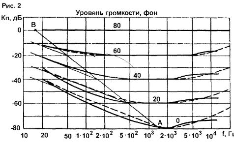
Likewise, relative to the equal loudness curve 80 von. the corrected frequency response is constructed at volume levels of 40. 20 and 0 (3) background and the family of frequency response of the volume control required for correct loudness is obtained. In the range of changes in the volume level of 80 dB, it is shown in Fig. 2 (solid thick lines).
Now it is necessary to build a thin-compensated volume controller, the frequency response of which approaches the required one the best way. In the frequency range below 2 kHz, the curve corresponding to the minimum gain can be approximated by the frequency response of an RC circuit. shown in Fig.3. This characteristic to the left of the inflection frequency f1 (Fig. 3b) has a slope of 6 dB per octave. If resistor R2 of this circuit is made variable, and its minimum resistance is chosen much less than R1. then when adjusting resistance R2, along with changing the transmission coefficient of the circuit, the inflection frequency of its frequency response will also change. As can be seen from Fig. 2, taking into account the approximation within 3 dB, the inflection frequency must move during the control process along the LP line in order to provide the required loudness compensation. The range of changes in resistance R2 cannot be more than 100, since fa/fb must change by 80 dB (10,000 times). The resistance R2 should change by the same amount.
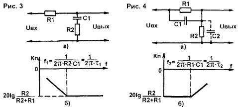
It is quite obvious that by changing the resistance of resistor R2 alone, it will not be possible to achieve such a shift in the inflection frequency and a change in the transmission coefficient. However, increasing the number of series-connected RC circuits and simultaneously reducing the adjustment limits of resistor R2 in each of them. this problem can be solved. Already two such RC circuits (the time constant of the second circuit should be 20...40 times greater than the first) allow us to obtain a completely acceptable result: the deviation of the curves of the real family of frequency response (dashed lines in Fig. 2) from the required one (solid line) does not exceed 3 dB.
At frequencies above 2 kHz, a decrease in volume from 80 to 60 von is accompanied by the appearance of an inflection in the 60 von curve at a frequency of 5 kHz with a slope of 3 dB per octave. With a further decrease in volume up to the threshold of auditory sensation (level 3 background), the inflection frequency shifts from 5 to 3 kHz, while the slope of the curves remains virtually unchanged. In this frequency range, curve 3 background can be approximated by the frequency response of the RC circuit shown in Fig. 4a. The values of resistors R1 and R2 here are the same as in the RC circuit. shown in Fig.3. A change in resistance R2 does not lead to a shift in the inflection frequency f2 (Fig. 4b).
To ensure that an increase in volume from 60 to 80 von is not accompanied by a rise in higher sound frequencies, the RC circuit must provide frequency compensation at the maximum transmission coefficient, which can be achieved by shunting resistor R2 with capacitor C2 of such a capacity that the equality of the time constants T2 = R1C1 and x3 is observed =R2-C2. In this case, the decrease in resistance R2 necessary for volume control will be accompanied by a decrease in the time constant TC and a shift in the cutoff frequency of the RC circuit (f3 = 1/2nR2-C2) to a higher frequency region, and the inflection frequency f2 will remain unchanged, which will ensure the required compliance The frequency response of an RC circuit is a curve of equal volume in the frequency range above 2 kHz.
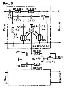
An example of the practical implementation of a fine-compensated volume control is shown in Fig. 5 (4, 5]. The resistances of the resistors and capacitors included in it can be calculated using the following relationships:
R1=R3=R:
R4min=R5min=0.01R;
R4max=R5max=10R;
R1C2=R3C3=20MKC;
R4minC4=4000 µs;
R5minC5=100 µs;
R5maxC6=20 µs. Resistance R can be selected within 103..106 Ohms. In Fig. 5 R=510 kOhm. R5minC5=2000 µs (4000); R4minC4=100 µs.
To avoid shunting the circuit R5-C5. The amplifier 34 connected to the output of the regulator must have a high input impedance and a small input capacitance. In particular, it can be implemented using a voltage follower circuit using an op-amp with field-effect transistors at the input. The output resistance of the amplifier connected in front of the regulator should be 20 times less than the resistance R2. The variable resistors of the thin-compensated volume control must be double. In our case, their functions are performed by photoresistors R4, R5, and resistor R10 serves as the control element. changing current through an incandescent lamp HL1. The SFZ-1 photoresistors used in the volume control have high speed (time constant - less than 0.06 s) and the required range of resistance changes. Incandescent lamp (subminiature) - NSM (6.3 Vx20 mA). the current through it varies within 6...18 mA. Photoresistors are placed close to the incandescent lamp, and the entire regulator is placed in a light-proof metal shield.
Figure 5 shows a two-channel control for a stereo amplifier. In it, it is necessary to select photoresistors in pairs in different channels so that when changing in the range from 104 to 106 Ohms, their resistances differ by no more than 20%. Otherwise, channel imbalance will be noticeable when changing the volume.
Stereo balance is adjusted by resistor R9 within ±6 dB. Capacitors C7, SV eliminate rustling and crackling sounds created by variable resistors.
Variable resistor R10 must have a linear regulation characteristic. Fixed resistors - with a resistance deviation from the nominal value of no more than ±5%. Capacitors C1. C4, C5 are paper MBMs, the rest are ceramic. The capacitance of capacitor C6 depends on the mounting capacitance and the input capacitance of the amplifier connected to the output of the volume control. Incandescent lamps must be powered from a stabilized power source.
Setting up the regulator comes down to ensuring the linearity of the frequency response at K„=0 dB (by selecting C6) and checking the identity of the family of its frequency response in different channels stereo amplifier at different volume levels.
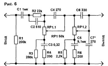
Another example of a controller is shown in Fig. 6. Here, dual variable resistors are used with a linear dependence of the resistance on the angle of rotation of the axis (group “A”). For a stereo regulator, you need to use two dual variable resistors. This solution does not cause any particular problems with adjusting the balance if volume level scales are applied to the panel where both resistors are installed.
An attempt to use a quad resistor encounters great difficulties; firstly, it is a very rare “bird” in our area, secondly, its resistors have large variations in resistance, and thirdly, an additional balance regulator is required, which does not simplify the entire design. The spread of resistance of dual resistors is quite acceptable for this circuit. If dual resistors have a different resistance, then the capacitances of the capacitors must be recalculated using the given ratios. Resistors R3 and R5 serve to stop the rise of low frequencies outside the audio range.
When the variable resistor sliders are in the upper position, the controller transmission coefficient is -6 dB. The adjustment range at a frequency of 2 kHz is 80...85 dB. Deviation from the required AMX is no more than ±2 dB. if the load resistance of the regulator is more than 1 MOhm, and the load capacitance is less than 50 pF. Capacitors C1. NW. C5 are film, the rest are mica. Adjusting the regulator - no adjustment at all!
And finally, I will say that if you only listen to loud music, then it is enough to have a level control with a control range of 10... 15 dB. But if you want to feel the charm of quiet music, as if coming from a nearby park, then build this volume control, you won’t regret it!
Literature
1. A. Nikitin. Volume control in Hi-Fi equipment. - Radiohobby, 2002. No. 2, p. 63.
2. Terekhov P. About volume control. - Radio, 1982, No. 9, P.42.
3. Zwicker E.. Feldkeller R. The ear as a receiver of information. - M.: Communication. 1971.
4. I. Pugachev. Loud volume control. - Radio, 1988. N911.C.35.
5 Copyright certificate of the USSR No. 1390776. - Bulletin "Discoveries, inventions...". 1988, no. 15.
I. PUGACHEV, Minsk.
In this article we will look at the circuit of an electronic volume control with remote control and digital level indication.
Fig.1. Front of the device
Fig.2. Back of the device
The volume is increased by button or remotely from the remote control (infrared control). Almost any home control panel is suitable.
The device diagram is shown in Figure 3.
Fig.3. Electrical circuit diagram
Audio level switching is based on the CD4017 decimal counter (DD1). This microcircuit has 10 outputs Q0-Q9. After power is applied to the circuit, a logical one is immediately present at the Q0 output, the HL1 LED lights up, indicating zero level sound. Resistors R4-R12, which have different resistances, are connected to the remaining outputs Q1-Q9.
Let me remind you that the microcircuit produces a signal at the same time high level only at one of its outputs, and sequential switching between them occurs when a short pulse is applied to the input (pin 14).
Based on this, the resistances in the group of resistors R4-R12 are selected in descending order (from top to bottom in the circuit), so that each time the microcircuit is switched, more and more current flows to the base of transistor VT2, gradually opening the transistor.
A signal from an external ULF or sound source is supplied to the collector of this transistor.
So, by switching the counter chip, we essentially change the collector-emitter resistance and thereby change the volume of the sound entering the speaker.
The resistance of the resistors depends on the gain of the transistor (h21e). For example, when using 2N3904, the resistance of resistor R4 can be about 3 kOhm in order to “open” the transistor a little, while the sound will be at the quietest level. And resistance R12 should be the smallest of the entire group (about 50 Ohms) to ensure saturation mode and maximum collector-emitter throughput, respectively, the maximum volume of this regulator.
It is difficult for me to indicate the specific ratings of R4-R12, since this still very much depends on the power of the audio signal supplied to the transistor, as well as on the power supply. It is best to use multi-turn trimming resistors and adjust the stages “by ear”.
At the bottom of the diagram there is an indication unit based on the K176ID2 (DD2) decoder. It is designed to control a seven-segment indicator.
A binary code is supplied to the decoder inputs, so an encoder is built on diodes VD1-VD15, which converts the decimal signal from CD4017 into a binary code understandable for K176ID2. This diode circuit may seem strange and archaic, but it is quite functional. Diodes should be selected with a low voltage drop, such as Schottky diodes. But in my case, ordinary silicon 1N4001 were used, they can be seen in Figure 2.
So, the signal from the counter output goes not only to the base of the transistor, but also to the diode converter, turning into binary code. Next, DD2 will accept a binary code and the seven-segment indicator will display the desired number indicating the sound level.
The K176ID2 microcircuit is convenient in that it allows the use of indicators with both a common cathode and a common anode. The second type is used in the scheme. Resistor R17 limits the current of the segments.
Resistors R13-R16 pull the decoder inputs to minus for stable operation.
Now let's look at the top left part of the diagram. The two-position switch SA1 sets the volume control mode. In the upper (according to the diagram) position of the SA1 key, the volume is changed manually by pressing the SB1 clock button. Capacitor C3 eliminates contact bounce. Resistor R2 pulls the CLK input to negative, preventing false alarms.
After power is applied, the HL1 LED lights up, and the indicator shows zero - this is silent mode (Figure 4, top).
Fig.4. Displaying levels on the indicator
By pressing the clock button, the speaker volume increases in small jumps from level 1 to level 9, the next press again activates the silent mode.
If you set the switch to the down position (according to the diagram), the DD1 input is connected to an infrared remote control circuit based on a TSOP receiver. When an external IR signal arrives at the TSOP receiver, a negative voltage appears at its output, unlocking transistor VT1. This transistor is any low-power PNP structure, for example KT361 or 2N3906.
I recommend choosing an IR receiver (IF1) with an operating frequency of 36 kHz, since it is at this frequency that most remote controls (for TV, DVD, etc.) operate. When you press any button on the remote control, the volume will be controlled.
The circuit contains a locking button SB2. While it is pressed, the reset pin RST is connected to the power supply minus and the counter will switch. Using this button, you can reset the counter and volume level to zero, and if you leave it in the off position, the reset pin will not be pulled to minus and the counter Not will receive signals from the remote control, and Not will respond to pressing the SB1 button.
Fig.5. Switches, a tact button and a TSOP receiver with wiring are located on a separate board
I supply the audio signal to the regulator transistor from an amplifier on a PAM8403 chip. The VT2 collector is connected to the positive output of one of the amplifier channels (R), and its emitter is connected to the positive terminal of the speaker (red wire in the photo). The negative terminal of the column (black and red) is connected to the negative of the channel being used. The sound source in my case is a mini mp3 player.
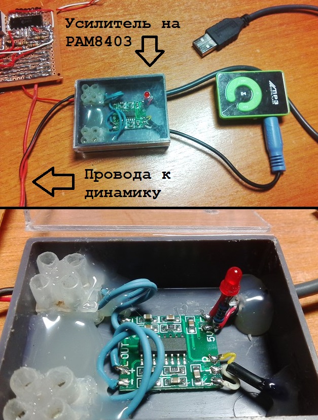
Fig.6. Connecting the device
Why are trim resistors used?
I would like to draw your attention to the photo of the back of the device (Fig. 2). There you can see that there are three 100 kOhm trimming resistors R4, R5, R6. I only implemented three volume levels because the remaining resistors (R7-R12) did not fit on the board. Trimmer resistors allow you to adjust volume levels for different sources sound, because they differ in audio signal strength.
Disadvantages of the device.
1) Volume control occurs only up in level, i.e. only louder. You won’t be able to decrease it right away; you will have to reach level 9 and then return to the initial level again.
2) The sound quality deteriorates slightly. The greatest distortion is present at quiet levels.
3) Does not control the stereo signal. The introduction of a second transistor for one more channel does not solve the problem, because The emitters of both transistors are combined at the minus power supply, which results in a “mono” sound.
Improvement of the scheme.
You can use a resistor optocoupler instead of a transistor. A fragment of the circuit is shown in Figure 7.
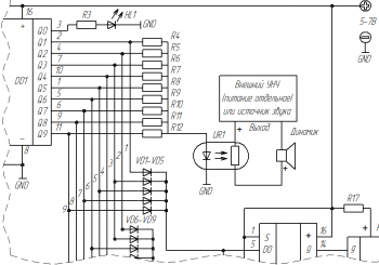
Fig.7. A fragment of the same circuit with an optocoupler
A resistor optocoupler consists of a light emitter and a light receiver connected optical communication. They are galvanically isolated, which means the control circuit should not interfere with the audio signal passing through the photoresistor. The photoresistor, under the influence of light from the emitter (LED or the like), will change its resistance and the volume will change. The optocoupler elements are galvanically isolated, which means that two or more audio signal channels can be controlled (Fig. 8).
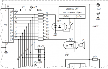
Fig.8. Control of two channels using resistor optocouplers
Resistors R4-R12 are selected individually.
The device can be powered from USB 5 Volt. As the voltage increases, the resistance of the current-limiting resistor R17 should be increased so that the seven-segment indicator HG1 does not fail, and the resistance of R1 should also be increased to protect the TSOP receiver. But I do not recommend exceeding the supply voltage above 7 Volts.
This article includes a video that outlines the principle of operation, shows the design assembled on the board, and tests this device.
List of radioelements
| Designation | Type | Denomination | Quantity | Note | Shop | My notepad | |
|---|---|---|---|---|---|---|---|
| Components for the circuit (Fig. 1) | |||||||
| DD1 | Special logic | CD4017B | 1 | Decimal counter | Search in LCSC | To notepad | |
| DD2 | Chip. Decoder | K176ID2 | 1 | Search in LCSC | To notepad | ||
| VT1 | Bipolar transistor | 2N3906 | 1 | Any low power PNP | Search in LCSC | To notepad | |
| VT2 | Bipolar transistor | 2N3904 | 1 | Possibly KT3102 | Search in LCSC | To notepad | |
| VD1-VD15 | Schottky diode | 1N5817 | 15 | Search in LCSC | To notepad | ||
| C1 | 47 - 100 µF | 1 | Search in LCSC | To notepad | |||
| C2 | Ceramic capacitor | 0.1 µF | 1 | Search in LCSC | To notepad | ||
| C3 | Electrolytic capacitor | 1 - 10 µF | 1 | Search in LCSC | To notepad | ||
| R1 | Resistor | 100 Ohm | 1 | Search in LCSC | To notepad | ||
| R2 | Resistor | 20 - 100 kOhm | 1 | Search in LCSC | To notepad | ||
| R3 | Resistor | 100 - 300 Ohm | 1 | Search in LCSC | To notepad | ||
| R4-R12 | Resistor | Pick up | 9 | Pick up | |||