Every radio amateur who regularly designs electronic devices, I think there is a regulated power supply at home. The thing is really convenient and useful, without which, once you try it in action, it becomes difficult to do without. Indeed, if we need to check, for example, an LED, we will need to set it precisely operating voltage, since if the voltage supplied to the LED is significantly exceeded, the latter may simply burn out. Also with digital circuits, set the output voltage on the multimeter to 5 volts, or any other voltage we need and go ahead.
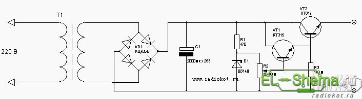
Many novice radio amateurs first assemble a simple adjustable power supply, without adjusting the output current and protecting against short circuit. So it was with me, about 5 years ago I assembled a simple power supply with only adjustable output voltage from 0.6 to 11 volts. Its diagram is shown in the figure below:
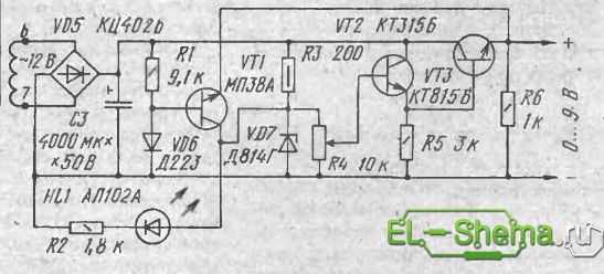
But a few months ago I decided to upgrade this power supply and add a small short circuit protection circuit to its circuit. I found this diagram in one of the issues of Radio magazine. Upon closer examination, it turned out that the circuit is in many ways reminiscent of the above circuit diagram of the power supply I assembled earlier. If there is a short circuit in the powered circuit, the short circuit LED goes out, signaling this, and the output current becomes equal to 30 milliamps. It was decided to take part of this scheme and supplement it with my own, which is what I did. The original diagram from Radio magazine, which includes an addition, is shown in the figure below:
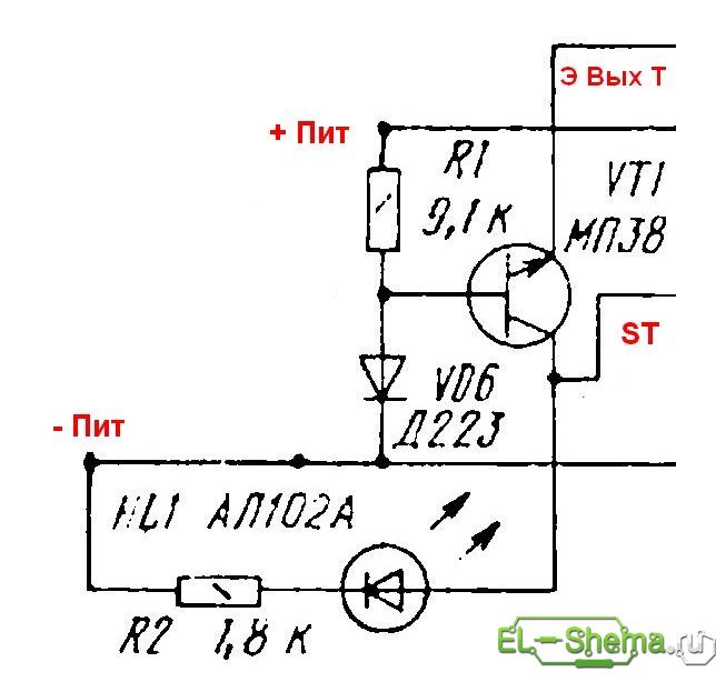
The following picture shows the part of this circuit that will need to be assembled.
The value of some parts, in particular resistors R1 and R2, needs to be recalculated upward. If anyone still has questions about where to connect the output wires from this circuit, I will provide the following figure:

I’ll also add that in the assembled circuit, regardless of whether it is the first circuit or the circuit from the Radio magazine, you must place a 1 kOhm resistor at the output, between plus and minus. In the diagram from Radio magazine this is resistor R6. All that remains is to etch the board and assemble everything together in the power supply case. Mirror boards in the program Sprint Layout no need. Short circuit protection circuit board drawing:

About a month ago I came across a diagram of an output current regulator attachment that could be used in conjunction with this power supply. I took it from this site. Then I assembled this set-top box in a separate case and decided to connect it as needed to charge batteries and similar actions where monitoring the output current is important. Here is the diagram of the set-top box, the transistor KT3107 in it was replaced with KT361.

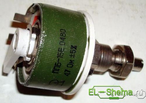
But later the idea came to me to combine, for convenience, all this in one building. I opened the power supply case and looked, there was not enough space left, the variable resistor would not fit. The current regulator circuit uses a powerful variable resistor, which has rather large dimensions. Here's what it looks like:
Then I decided to simply connect both cases with screws, making the connection between the boards with wires. I also set the toggle switch to two positions: output with adjustable current and unregulated. In the first case, the output from the main board of the power supply was connected to the input of the current regulator, and the output of the current regulator went to the clamps on the power supply case, and in the second case, the clamps were connected directly to the output from the main board of the power supply. All this was switched with a six-pin toggle switch in 2 positions. Here is a drawing of the current regulator printed circuit board:

In the figure of the printed circuit board, R3.1 and R3.3 pins are indicated variable resistor first and third, counting from the left. If anyone wants to repeat it, here is a diagram for connecting a toggle switch for switching:
![]()
Printed circuit boards of the power supply, protection circuits and current control circuits are attached in the archive. Material prepared by AKV.
This diagram represents simplest block power supply on transistors, equipped with short circuit protection (short circuit). Its diagram is shown in the figure.
Main parameters:
- Output voltage - 0..12V;
- The maximum output current is 400 mA.
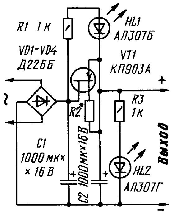
The scheme works as follows. The input voltage of the 220V network is converted by a transformer to 16-17V, then rectified by diodes VD1-VD4. Filtering of rectified voltage ripples is carried out by capacitor C1. Next, the rectified voltage is supplied to the zener diode VD6, which stabilizes the voltage at its terminals to 12V. The remainder of the voltage is extinguished by resistor R2. Next, the voltage is adjusted by variable resistor R3 to the required level within 0-12V. This is followed by a current amplifier on transistors VT2 and VT3, which amplifies the current to a level of 400 mA. The load of the current amplifier is resistor R5. Capacitor C2 additionally filters output voltage ripple.
This is how protection works. In the absence of a short circuit at the output, the voltage at the terminals of VT1 is close to zero and the transistor is closed. Circuit R1-VD5 provides a bias at its base at a level of 0.4-0.7 V (voltage drop across open p-n diode transition). This bias is enough to open the transistor at a certain collector-emitter voltage level. As soon as a short circuit occurs at the output, the collector-emitter voltage becomes different from zero and equal to the voltage at the output of the unit. Transistor VT1 opens, and the resistance of its collector junction becomes close to zero, and, therefore, at the zener diode. Thus, zero input voltage is supplied to the current amplifier; very little current will flow through transistors VT2, VT3, and they will not fail. The protection is turned off immediately when the short circuit is eliminated.
Details
The transformer can be any with a core cross-sectional area of 4 cm 2 or more. The primary winding contains 2200 turns of PEV-0.18 wire, the secondary winding contains 150-170 turns of PEV-0.45 wire. A ready-made frame scan transformer from old tube TVs of the TVK110L2 series or similar will also work. Diodes VD1-VD4 can be D302-D305, D229Zh-D229L or any with a current of at least 1 A and a reverse voltage of at least 55 V. Transistors VT1, VT2 can be any low-frequency low-power ones, for example, MP39-MP42. You can also use more modern silicon transistors, for example, KT361, KT203, KT209, KT503, KT3107 and others. As VT3 - germanium P213-P215 or more modern silicon high-power low-frequency KT814, KT816, KT818 and others. When replacing VT1, it may turn out that short-circuit protection does not work. Then you should connect another diode (or two, if necessary) in series with VD5. If VT1 is made of silicon, then it is better to use silicon diodes, for example, KD209(A-B).
In conclusion, it is worth noting that instead of those indicated in p-n-p scheme transistors can be used with similar parameters npn transistors(not instead of any of VT1-VT3, but instead of all of them). Then you will need to change the polarity of the diodes, zener diode, capacitors, diode bridge. At the output, accordingly, the polarity of the voltage will be different.
List of radioelements
| Designation | Type | Denomination | Quantity | Note | Shop | My notepad |
|---|---|---|---|---|---|---|
| VT1, VT2 | Bipolar transistor | MP42B | 2 | MP39-MP42, KT361, KT203, KT209, KT503, KT3107 | Search in Fivel | To notepad |
| VT3 | Bipolar transistor | P213B | 1 | P213-P215, KT814, KT816, KT818 | Search in Fivel | To notepad |
| VD1-VD4 | Diode | D242B | 4 | D302-D305, D229Zh-D229L | Search in Fivel | To notepad |
| VD5 | Diode | KD226B | 1 | Search in Fivel | To notepad | |
| VD6 | Zener diode | D814D | 1 |
The connection diagram of the transistor to the power supply is shown in Fig. 1, and the current-voltage characteristics of the transistor for various resistances of resistor R1 are shown in Fig. 2. This is how protection works. If the resistance of the resistor is zero (i.e., the source is connected to the gate), and the load consumes a current of about 0.25 A, then the voltage drop across the field-effect transistor does not exceed 1.5 V, and practically all of the rectified voltage will be across the load. When a short circuit appears in the load circuit, the current through the rectifier increases sharply and, in the absence of a transistor, can reach several amperes. The transistor limits the short circuit current to 0.45...0.5 A, regardless of the voltage drop across it. In this case, the output voltage will become zero, and all the voltage will drop across the field-effect transistor. Thus, in the event of a short circuit, the power consumed from the power source will increase by in this example no more than doubled, which in most cases is quite acceptable and will not affect the “health” of the power supply parts.
Rice. 2
The short circuit current can be reduced by increasing the resistance of resistor R1. It is necessary to select a resistor such that the short circuit current is approximately twice the maximum load current.
This type of protection is especially convenient for power supplies with a smoothing RC filter - then the field-effect transistor is switched on instead of the filter resistor (such an example is shown in Fig. 3).
Since during a short circuit almost all of the rectified voltage drops across the field-effect transistor, it can be used for light or sound alarm. Here, for example, is a diagram for turning on the light alarm - Fig. 7. When everything is in order with the load, the green HL2 LED lights up. In this case, the voltage drop across the transistor is not enough to light the HL1 LED. But as soon as a short circuit appears in the load, the HL2 LED goes out, but the red HL1 flashes.
Rice. 3
Resistor R2 is selected depending on the desired short-circuit current limitation according to the recommendations made above.
The connection diagram for the sound alarm is shown in Fig. 4. It can be connected either between the drain and source of the transistor, or between the drain and gate, like the HL1 LED.
When sufficient voltage appears on the signaling device, the AF generator, made on a unijunction transistor VT2, comes into operation, and a sound is heard in the headphone BF1.
The unijunction transistor can be KT117A-KT117G, the telephone can be low-impedance (can be replaced with a low-power dynamic head).

Rice. 4
It remains to add that for low-current loads, a short-circuit current limiter using a field-effect transistor KP302V can be inserted into the power supply. When choosing a transistor for other blocks, you should take into account its permissible power and drain-source voltage.
Of course, such automation can also be introduced into a stabilized power supply that does not have short-circuit protection in the load.
Almost every novice radio amateur strives at the beginning of his creativity to design a network power supply in order to subsequently use it to power various experimental devices. And of course, I would like this power supply to “tell” about the danger of failure of individual components due to installation errors or malfunctions.
Today there are many schemes, including those with indication of a short circuit at the output. In most cases, such an indicator is usually an incandescent lamp connected to the load break. But with such inclusion we increase input impedance power source or, more simply put, we limit the current, which in most cases is, of course, acceptable, but not at all desirable.
The circuit shown in Fig. 1 not only signals a short circuit without affecting the output impedance of the device at all, but also automatically turns off the load when the output is shorted. In addition, LED HL1 reminds that the device is plugged in, and HL2 lights up when fuse FU1 blows, indicating the need to replace it.
Electric circuit diagram homemade power supply with short circuit protection
Consider the operation of a homemade power supply. The alternating voltage removed from the secondary winding T1 is rectified by diodes VD1...VD4, assembled in a bridge circuit. Capacitors C1 and C2 prevent the penetration of high-frequency interference into the network, and the oxide capacitor C3 smoothes out the voltage ripples supplied to the input of the compensation stabilizer, assembled at VD6, VT2, VT3 and providing a stable output voltage of 9 V.
The stabilization voltage can be changed by selecting the VD6 zener diode, for example, with KS156A it will be 5 V, with D814A - 6 V, with DV14B - V V, with DV14G -10 V, with DV14D -12 V. If desired, the output voltage can be made adjustable, To do this, a variable resistor with a resistance of 3-5 kOhm is connected between the anode and cathode VD6, and the base VT2 is connected to the motor of this resistor.
Let's consider the operation of the power supply protective device. The short circuit protection unit in the load consists of germanium p-p-p transistor VT1, electromagnetic relay K1, resistor R3 and diode VD5. The latter in this case serves as a stabistor that maintains a constant voltage of about 0.6 - 0.7 V based on VT1 relative to the total.
In normal mode of operation of the stabilizer, the transistor of the protection unit is securely closed, since the voltage at its base relative to the emitter is negative. When a short circuit occurs, the emitter of VT1, like the emitter of the regulating VT3, is connected to the common negative wire of the rectifier.
In other words, the voltage at its base relative to the emitter becomes positive, as a result of which VT1 opens, K1 is triggered and turns off the load with its contacts, and the HL3 LED lights up. After eliminating the short circuit, the bias voltage at the emitter junction VT1 again becomes negative and it closes, relay K1 is de-energized, connecting the load to the output of the stabilizer.
Parts for making a power supply. Any electromagnetic relay with the lowest possible operating voltage. In any case, one thing must be observed an indispensable condition: the secondary winding T1 must produce a voltage equal to the sum of the stabilization and relay response voltages, i.e. if the stabilization voltage, as in this case, is 9 V, and U of the relay is 6 V, then the secondary winding must have at least 15 V, but not exceed the permissible value at the collector-emitter of the transistor used. The author used TVK-110L2 as T1 on the prototype. Printed circuit board device is shown in Fig. 2.
Power supply circuit board
Prus S.V.
I was inspired to create this article by my experience in creating power supplies and chargers based on simple switching power supplies, which are both SMPS based on IR2153 and a converted different ways for power supply electronic transformer. These power supplies are simple, unstabilized switching power supplies without any protection. Despite these disadvantages, such power supplies are quite simple to manufacture, do not require complex configuration, and the time required to create such a power supply is less than for a full PWM power supply with stabilization and protection units.
By combining such a power supply and a simple PWM regulator on the NE555, we get an adjustable power supply both for experiments and for charging the battery. There is no limit to our joy until we try this device for a spark, or mistakenly, while thinking about creating the next device, mix up the polarity of the battery being charged. Shouting out with a loud bang and spraying acrid smoke into the room in which this embarrassment took place, the invention tells us that simple pulse block power supply, which is assembled according to a simplified introductory diagram cannot be reliable.
Then the idea came to find not just to introduce this or that protection unit into a specific instance of the power supply, but to find or create a universal high-speed circuit that can be implemented in any secondary power source.
Requirements for the protection unit:
Minimum details
The protection board should take up little space
Operable at high load currents
No relay
High response speed
One of the options that interested me was this diagram, found on the Internet:
When the output of this circuit is closed, the gate capacitance VT1 is discharged through the diode VD1, which leads to the closure of VT1 and no current flows through the transistor, the power supply remains safe and sound. But what happens if you connect a 300W load to the output of this circuit, when our power supply can only output 200W? Despite the fact that we have a protection circuit, the tortured power supply explodes again.
Disadvantages of this scheme:
1. It is necessary to accurately select the shunt resistance so that the maximum permissible current of the power supply creates such a voltage drop on the selected shunt that VT2, when opening, completely closes VT1.
2. In this circuit, there may come a time when the current passing through the shunt slightly opens VT2, as a result of which VT1 begins to close and remains in such a state that it will not be closed, and given that a considerable current flows through VT1, this linear mode will cause it to overheat severely , as a result of which VT1 will be broken.
I once used trigger protection in a power supply on IR2153, and was pleased with its performance. Let's attach a shunt to the trigger latch circuit on a complementary pair of transistors as a current sensor and an n-channel transistor as key element we get the following diagram:
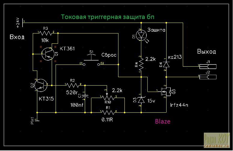
After power is applied to the circuit, transistor Q3, through the LED and R4, opens, the zener diode D3 limits the gate voltage field effect transistor. D4 protects Q3 from emissions high voltage, when connecting an inductive load (electric motor). An analogue of a thyristor is assembled on a pair of transistors Q1, Q2. The current flowing through the shunt R1 causes a voltage drop, which from the motor of the variable resistor R10, and the circuit R2, C2, goes to the base of the transistor Q2. The amount of voltage from the shunt, which is proportional to the current flowing through this shunt, can be adjusted with a variable resistor R10. At the moment when the voltage at the base of Q2 becomes greater than 0.5-0.7V, transistor Q2 will begin to open, thereby opening Q1, in turn, transistor Q1, opening, will open Q2. This process happens very quickly, in a split second the transistors will open each other and remain in such a stable state. Through the open analogue of the thyristor, gate Q3, as well as resistor R4, will be connected to the common conductor of the circuit, which will lead to the closing of Q3 and the lighting of LED D1 will indicate that the protection has tripped. You can remove the protection either by briefly turning off the power or by briefly pressing the S1 button.
A universal protection circuit was created and tested in operation; shunt R1 was made up of two 0.22 Ohm 5W resistors. Remained last step- we introduce protection against polarity reversal of the battery terminals into the new circuit.
Circuit with reverse polarity protection:
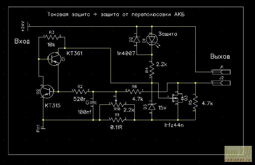
Our circuit was supplemented with diode D2 and resistors R6, R5. Button S1 was removed from the circuit due to the fact that when the protection was triggered, it did not remove the circuit from protection after modification.
Current protection remains unchanged; the protection can be removed by turning off the power for 2-3 seconds. When connected to the output of the battery circuit, reversing the polarity, the voltage from the battery through diode D2, resistor R6 goes to the base of Q2, protection Q3 is triggered, the LED D1 signals that the protection has tripped.
On this wave, I am finishing my search for protection for my simple IP. I am satisfied with the performance of my circuits, I hope they will be useful to you too.
Enjoy your experiments!
ID: 2237
|
What do you think of this article? |